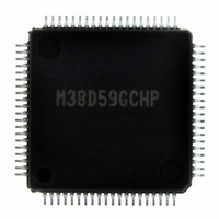
M38D59GCHP#U0 Renesas Electronics America, M38D59GCHP#U0 Datasheet - Page 38

M38D59GCHP#U0
Manufacturer Part Number
M38D59GCHP#U0
Description
IC 740/38D5 MCU QZ-ROM 80LQFP
Manufacturer
Renesas Electronics America
Series
740/38000r
Datasheet
1.M38D58G8FPU0.pdf
(144 pages)
Specifications of M38D59GCHP#U0
Core Processor
740
Core Size
8-Bit
Speed
12.5MHz
Connectivity
SIO, UART/USART
Peripherals
LCD, LED, PWM, WDT
Number Of I /o
59
Program Memory Size
48KB (48K x 8)
Program Memory Type
QzROM
Ram Size
2K x 8
Voltage - Supply (vcc/vdd)
1.8 V ~ 5.5 V
Data Converters
A/D 8x10b
Oscillator Type
Internal
Operating Temperature
-20°C ~ 85°C
Package / Case
80-LQFP
Lead Free Status / RoHS Status
Lead free / RoHS Compliant
Eeprom Size
-
Available stocks
Company
Part Number
Manufacturer
Quantity
Price
38D5 Group
Rev.3.04
REJ03B0158-0304
• Frequency Divider For Timer
Timer 1, timer 2, timer 3 and timer 4 have the frequency divider
for the count source. The count source of the frequency divider is
switched to X
4 in the on-chip oscillator mode by the CPU mode register. The
frequency divider is controlled by each timer division ratio
selection bit. The division ratio can be selected from as follows;
1/1, 1/2, 1/16, 1/256 of f(X
frequency division or count source* while the timer count is
stopped.
*This also applies when the frequency divider output is selected
• Timer 1, Timer 2
The count source for timer 1 and timer 2 can be set using the
timer 12 mode register. X
source. If X
of whether or not the X
is operating. In addition, the timer 12 mode register can be used
to output from the P7
every time timer 2 underflows.
At reset, all bits of the timer 12 mode register are set to “0”, timer
1 is set to “FF
When executing the STP instruction, previously set the wait time
at return.
• Timer 3, Timer 4
The count sources of timer 3 and timer 4 can be selected by
setting the timer 34 mode register. Also, by the timer 34 mode
register, each time timer 3 or timer 4 underflows, the signal of
which polarity is inverted can be output from P7
P7
Fig. 26 Waveform of PWM0 and PWM1
as the timer count source and the count source is switched in
conjunction with a transition between operating modes (on-
chip oscillator mode, X
careful when changing settings in the CPU mode register.
4
/T
4OUT
pin.
CIN
PWM01 register = “00
PWM01 register = “01
PWM01 register = “10
PWM01 register = “11
IN
16
May 20, 2008 Page 36 of 134
n: Setting value of Timer 3 or Timer 4
ts: One period of Timer 3 count source or Timer 4 count source
PWM01 register (address 0024
is selected, count operation is possible regardless
”, and timer 2 is set to “01
, X
Output waveform of Timer 3 PWM0 or Timer 4 PWM1
CIN
2
, or the on-chip oscillator OCO divided by
IN
/T
2OUT
input oscillator or the on-chip oscillator
IN
IN
CIN
), f(X
mode, or low-speed mode). Be
pin a signal to invert the polarity
Interrupt request
may be selected as the count
CIN
2
2
2
2
”
”
”
”
) or f(OCO)/4. Switch the
(n+1) × ts
(n+1) × ts
(n+1) × ts
16
n × ts
Short interval
”.
256 ×
16
) : 2-bit value corresponding to PWM0 (bits 0, 1) or PWM1 (bits 2, 3)
3
/T
t
s
3OUT
(n+1) × ts
pin or
n × ts
n × ts
n × ts
Short interval
256 ×
• Timer 3 PWM
A PWM rectangular waveform corresponding to the 10-bit
accuracy can be output from the P7
pin by setting the timer 34 mode register and PWM01 register
(refer to Figure 26).
One output pulse is the short interval. Four output pulses are the
long interval. The “n” is the value set in the timer 3 (address
0022
timer 3 or timer 4 count source. “H” width of the short interval is
obtained by n × ts.
However, in the long interval, “H” width of output pulse is
extended for ts which is set by the PWM01 register (address
0024
<Notes on Timer 1 to Timer 4>
(1) Timer 3 PWM
• When PWM output is suspended after starting PWM output,
• In the PWM mode, the follows are performed every cycle of
(2) Write to Timer 2, Timer 3, Timer 4
When writing to the latch only, if the write timing to the reload
latch and the underflow timing are almost the same, the value is
set into the timer and the timer latch at the same time. In this
time, counting is stopped during writing to the reload latch.
Long interval
4 × 256 ×
depending on the level of the output pulse at that time to
resume an output, the delay of the one section of the short
interval may be needed.
the long interval (4 × 256 × ts).
t
s
Stop at “H”: No output delay
Stop at “L”: Output is delayed time of 256 × ts
• Generation of timer 3, timer 4 interrupt requests
• Update of timer 3, timer 4
16
16
) or the timer 4 (address 0023
).
(n+1) × ts
(n+1) × ts
n × ts
n × ts
Short interval
t
s
256 ×
0
Mode, Timer 4 PWM
t
s
0
Mode, Timer 4 PWM
n × ts
n × ts
n × ts
n × ts
Short interval
256 ×
Interrupt request
3
16
/PWM
t
s
). The “ts” is one period of
1
0
Mode
pin and P7
1
Mode
4
/PWM
1


