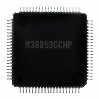
M38D59GCHP#U0 Renesas Electronics America, M38D59GCHP#U0 Datasheet - Page 51

M38D59GCHP#U0
Manufacturer Part Number
M38D59GCHP#U0
Description
IC 740/38D5 MCU QZ-ROM 80LQFP
Manufacturer
Renesas Electronics America
Series
740/38000r
Datasheet
1.M38D58G8FPU0.pdf
(144 pages)
Specifications of M38D59GCHP#U0
Core Processor
740
Core Size
8-Bit
Speed
12.5MHz
Connectivity
SIO, UART/USART
Peripherals
LCD, LED, PWM, WDT
Number Of I /o
59
Program Memory Size
48KB (48K x 8)
Program Memory Type
QzROM
Ram Size
2K x 8
Voltage - Supply (vcc/vdd)
1.8 V ~ 5.5 V
Data Converters
A/D 8x10b
Oscillator Type
Internal
Operating Temperature
-20°C ~ 85°C
Package / Case
80-LQFP
Lead Free Status / RoHS Status
Lead free / RoHS Compliant
Eeprom Size
-
Available stocks
Company
Part Number
Manufacturer
Quantity
Price
- Current page: 51 of 144
- Download datasheet (3Mb)
38D5 Group
Rev.3.04
REJ03B0158-0304
[Serial I/O2 Operation]
Writing to the serial I/O2 register initializes the serial I/O2
counter to “7”.
After writing, the S
synchronous clock changes from “H” to “L”. The S
captures data each time the synchronous clock changes from “L”
to “H” and the serial I/O2 register shifts 1-bit simultaneously.
When the external clock is selected as the synchronous clock,
counting the synchronous clock eight times results the following:
After transfer is completed, the S
impedance state.
Fig. 40 Serial I/O2 timing
Notes 1: When the internal clock is selected as the transfer, the dividing frequency of internal clock for transfer
Serial I/O2 output S
• Serial I/O2 counter = “0”
• Synchronous clock is stopped at “H”
• Serial I/O2 interrupt request bit = “1”
Reception enable signal
(When the internal clock
Serial I/O2 input S
Serial I/O2 register
2: When the internal clock is selected as the synchronous clock, the S
3: When the external clock is selected as the synchronous clock, the S
clock can be selected by bits 0 to 2 of serial I/O2 control register.
impedance state after transfer is completed.
after transfer is completed.
However, if the synchronous clock is continuously input, the serial I/O2 register continues shifting and the
S
OUT2
Transfer clock
May 20, 2008 Page 49 of 134
is selected)
write signal
pin keeps outputting transmit data.
S
RDY2
OUT2
OUT2
IN2
(1)
pin outputs data each time the
OUT2
pin is placed in the high-
D
0
D
IN2
1
pin
D
2
When the external clock is selected as the synchronous clock,
counting the synchronous clock eight times sets the serial I/O2
bit to “1” and the S
However, if the synchronous clock is continuously input, the
serial I/O2 register continues shifting and the S
outputting transmit data.
OUT2
OUT2
D
3
pin is placed in the high
pin retains the D
D
4
OUT2
7
pin retains the D7 output level.
D
Serial I/O2 interrupt request bit set
output level
5
D
6
D
OUT2
7
(2) (3)
pin keeps
Related parts for M38D59GCHP#U0
Image
Part Number
Description
Manufacturer
Datasheet
Request
R

Part Number:
Description:
KIT STARTER FOR M16C/29
Manufacturer:
Renesas Electronics America
Datasheet:

Part Number:
Description:
KIT STARTER FOR R8C/2D
Manufacturer:
Renesas Electronics America
Datasheet:

Part Number:
Description:
R0K33062P STARTER KIT
Manufacturer:
Renesas Electronics America
Datasheet:

Part Number:
Description:
KIT STARTER FOR R8C/23 E8A
Manufacturer:
Renesas Electronics America
Datasheet:

Part Number:
Description:
KIT STARTER FOR R8C/25
Manufacturer:
Renesas Electronics America
Datasheet:

Part Number:
Description:
KIT STARTER H8S2456 SHARPE DSPLY
Manufacturer:
Renesas Electronics America
Datasheet:

Part Number:
Description:
KIT STARTER FOR R8C38C
Manufacturer:
Renesas Electronics America
Datasheet:

Part Number:
Description:
KIT STARTER FOR R8C35C
Manufacturer:
Renesas Electronics America
Datasheet:

Part Number:
Description:
KIT STARTER FOR R8CL3AC+LCD APPS
Manufacturer:
Renesas Electronics America
Datasheet:

Part Number:
Description:
KIT STARTER FOR RX610
Manufacturer:
Renesas Electronics America
Datasheet:

Part Number:
Description:
KIT STARTER FOR R32C/118
Manufacturer:
Renesas Electronics America
Datasheet:

Part Number:
Description:
KIT DEV RSK-R8C/26-29
Manufacturer:
Renesas Electronics America
Datasheet:

Part Number:
Description:
KIT STARTER FOR SH7124
Manufacturer:
Renesas Electronics America
Datasheet:

Part Number:
Description:
KIT STARTER FOR H8SX/1622
Manufacturer:
Renesas Electronics America
Datasheet:

Part Number:
Description:
KIT DEV FOR SH7203
Manufacturer:
Renesas Electronics America
Datasheet:


