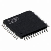
P89CV51RD2FBC,557 NXP Semiconductors, P89CV51RD2FBC,557 Datasheet - Page 38

P89CV51RD2FBC,557
Manufacturer Part Number
P89CV51RD2FBC,557
Description
IC 80C51 MCU FLASH 64K 44-TQFP
Manufacturer
NXP Semiconductors
Series
89Cr
Datasheet
1.P89CV51RB2FA512.pdf
(76 pages)
Specifications of P89CV51RD2FBC,557
Core Processor
8051
Core Size
8-Bit
Speed
40MHz
Connectivity
EBI/EMI, SPI, UART/USART
Peripherals
POR, PWM, WDT
Number Of I /o
32
Program Memory Size
64KB (64K x 8)
Program Memory Type
FLASH
Ram Size
1K x 8
Voltage - Supply (vcc/vdd)
4.5 V ~ 5.5 V
Oscillator Type
Internal
Operating Temperature
-40°C ~ 85°C
Package / Case
44-TQFP, 44-VQFP
Processor Series
P89CV5x
Core
80C51
Data Bus Width
8 bit
Data Ram Size
1 KB
Interface Type
SPI, UART
Maximum Clock Frequency
40 MHz
Number Of Programmable I/os
32
Number Of Timers
3
Operating Supply Voltage
4.5 V to 5.5 V
Maximum Operating Temperature
+ 85 C
Mounting Style
SMD/SMT
3rd Party Development Tools
PK51, CA51, A51, ULINK2
Minimum Operating Temperature
- 40 C
Cpu Family
89C
Device Core
80C51
Device Core Size
8b
Frequency (max)
40MHz
Total Internal Ram Size
1KB
# I/os (max)
32
Number Of Timers - General Purpose
3
Operating Supply Voltage (typ)
5V
Operating Supply Voltage (max)
5.5V
Operating Supply Voltage (min)
4.5V
Instruction Set Architecture
CISC
Operating Temp Range
-40C to 85C
Operating Temperature Classification
Industrial
Mounting
Surface Mount
Pin Count
44
Package Type
TQFP
Lead Free Status / RoHS Status
Lead free / RoHS Compliant
Eeprom Size
-
Data Converters
-
Lead Free Status / Rohs Status
Details
Other names
568-4257
935284103557
P89CV51RD2FBC
935284103557
P89CV51RD2FBC
Available stocks
Company
Part Number
Manufacturer
Quantity
Price
Company:
Part Number:
P89CV51RD2FBC,557
Manufacturer:
NXP Semiconductors
Quantity:
10 000
NXP Semiconductors
P89CV51RB2_RC2_RD2_3
Product data sheet
6.6.6 More about UART Mode 1
6.6.7 More about UART Modes 2 and 3
6.6.8 Multiprocessor communications
Reception is initiated by a detected 1-to-0 transition at RXD. For this purpose RXD is
sampled at a rate of 16 times whatever baud rate has been established. When a transition
is detected, the divide-by-16 counter is immediately reset to align its roll-overs with the
boundaries of the incoming bit times.
The 16 states of the counter divide each bit time into 16ths. At the 7th, 8th, and 9th
counter states of each bit time, the bit detector samples the value of RXD. The value
accepted is the value that was seen in at least 2 of the 3 samples. This is done for noise
rejection. If the value accepted during the first bit time is not 0, the receive circuits are
reset and the unit goes back to looking for another 1-to-0 transition. This is to provide
rejection of false start bits. If the start bit proves valid, it is shifted into the input shift
register, and reception of the rest of the frame will proceed.
The signal to load SBUF and RB8, and to set RI, will be generated if, and only if, the
following conditions are met at the time the final shift pulse is generated: (a) RI = 0, and
(b) either SM2 = 0, or the received stop bit = 1.
If either of these two conditions is not met, the received frame is irretrievably lost. If both
conditions are met, the stop bit goes into RB8, the 8 data bits go into SBUF, and RI is
activated.
Reception is performed in the same manner as in Mode 1.
The signal to load special function register SBUF and RB8, and to set RI, will be
generated if, and only if, the following conditions are met at the time the final shift pulse is
generated: (a) RI = 0, and (b) either SM2 = 0, or the received 9th data bit = 1.
If either of these conditions is not met, the received frame is irretrievably lost, and RI is not
set. If both conditions are met, the received 9th data bit goes into RB8, and the first 8 data
bits go into SBUF.
UART modes 2 and 3 have a special provision for multiprocessor communications. In
these modes, 9 data bits are received or transmitted. When data is received, the 9th bit is
stored in RB8. The UART can be programmed so that when the stop bit is received, the
serial port interrupt will be activated only if RB8 = 1. This feature is enabled by setting bit
SM2 in SCON. One way to use this feature in multiprocessor systems is as follows:
When the master processor wants to transmit a block of data to one of several slaves, it
first sends out an address byte which identifies the target slave. An address byte differs
from a data byte: the 9th bit is 1 in an address byte and 0 in a data byte. With SM2 = 1, no
slave will be interrupted by a data byte, i.e. the received 9th bit is 0. However, an address
byte having the 9th bit set to 1 will interrupt all slaves, so that each slave can examine the
received byte to see if it is being addressed or not. The addressed slave will clear its SM2
bit and prepare to receive the data (still 9 bits long) that follow. The slaves that were not
addressed leave their SM2 bits set and ignore the subsequent data bytes.
Rev. 03 — 25 August 2009
P89CV51RB2/RC2/RD2
80C51 with 1 kB RAM, SPI
© NXP B.V. 2009. All rights reserved.
38 of 76


