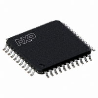
P89CV51RD2FBC,557 NXP Semiconductors, P89CV51RD2FBC,557 Datasheet - Page 13

P89CV51RD2FBC,557
Manufacturer Part Number
P89CV51RD2FBC,557
Description
IC 80C51 MCU FLASH 64K 44-TQFP
Manufacturer
NXP Semiconductors
Series
89Cr
Datasheet
1.P89CV51RB2FA512.pdf
(76 pages)
Specifications of P89CV51RD2FBC,557
Core Processor
8051
Core Size
8-Bit
Speed
40MHz
Connectivity
EBI/EMI, SPI, UART/USART
Peripherals
POR, PWM, WDT
Number Of I /o
32
Program Memory Size
64KB (64K x 8)
Program Memory Type
FLASH
Ram Size
1K x 8
Voltage - Supply (vcc/vdd)
4.5 V ~ 5.5 V
Oscillator Type
Internal
Operating Temperature
-40°C ~ 85°C
Package / Case
44-TQFP, 44-VQFP
Processor Series
P89CV5x
Core
80C51
Data Bus Width
8 bit
Data Ram Size
1 KB
Interface Type
SPI, UART
Maximum Clock Frequency
40 MHz
Number Of Programmable I/os
32
Number Of Timers
3
Operating Supply Voltage
4.5 V to 5.5 V
Maximum Operating Temperature
+ 85 C
Mounting Style
SMD/SMT
3rd Party Development Tools
PK51, CA51, A51, ULINK2
Minimum Operating Temperature
- 40 C
Cpu Family
89C
Device Core
80C51
Device Core Size
8b
Frequency (max)
40MHz
Total Internal Ram Size
1KB
# I/os (max)
32
Number Of Timers - General Purpose
3
Operating Supply Voltage (typ)
5V
Operating Supply Voltage (max)
5.5V
Operating Supply Voltage (min)
4.5V
Instruction Set Architecture
CISC
Operating Temp Range
-40C to 85C
Operating Temperature Classification
Industrial
Mounting
Surface Mount
Pin Count
44
Package Type
TQFP
Lead Free Status / RoHS Status
Lead free / RoHS Compliant
Eeprom Size
-
Data Converters
-
Lead Free Status / Rohs Status
Details
Other names
568-4257
935284103557
P89CV51RD2FBC
935284103557
P89CV51RD2FBC
Available stocks
Company
Part Number
Manufacturer
Quantity
Price
Company:
Part Number:
P89CV51RD2FBC,557
Manufacturer:
NXP Semiconductors
Quantity:
10 000
NXP Semiconductors
P89CV51RB2_RC2_RD2_3
Product data sheet
6.2.1 Expanded data RAM addressing
6.2 Memory organization
The various P89CV51RB2/RC2/RD2 memory spaces are as follows:
The P89CV51RB2/RC2/RD2 have 1 kB of data RAM; see
To access the expanded RAM (XRAM), the EXTRAM bit must be set and MOVX
instructions must be used. The expanded memory is physically located on the chip and
logically occupies the first bytes of external memory (addresses 000H to 2FFH).
Table 5.
Not bit addressable; reset value 00H.
When EXTRAM = 0, the expanded RAM is indirectly addressed using the MOVX
instruction in combination with any of the registers R0, R1 of the selected bank or DPTR.
Accessing the expanded RAM does not affect ports P0, P3[6] (WR), P3[7] (RD), or P2.
With EXTRAM = 0, the expanded RAM can be accessed as in the following example.
Expanded RAM access (indirect addressing only):
Bit
Symbol
•
•
•
•
•
MOVX @DPTR, A; DPTR contains 0A0H
DATA
128 B of internal data memory space (00H:7FH) accessed via direct or indirect
addressing, using instructions other than MOVX and MOVC. All or part of the stack
may be in this area.
IDATA
Indirect Data. 256 B of internal data memory space (00H:FFH) accessed via indirect
addressing using instructions other than MOVX and MOVC. All or part of the stack
may be in this area. This area includes the DATA area and the 128 B immediately
above it.
SFR
Special Function Registers. Selected CPU registers and peripheral control and status
registers, accessible only via direct addressing.
XDATA
‘External’ Data or auxiliary RAM. Duplicates the classic 80C51 64 kB memory space
addressed via the MOVX instruction using the DPTR, R0, or R1. The
P89CV51RB2/RC2/RD2 have 768 B of on-chip XDATA memory.
CODE
64 kB of code memory space, accessed as part of program execution and via the
MOVC instruction. The P89CV51RB2/RC2/RD2 have 16/32/64 kB of on-chip code
memory.
AUXR - Auxiliary function register (address 8EH) bit allocation
7
-
Rev. 03 — 25 August 2009
6
-
5
-
P89CV51RB2/RC2/RD2
4
-
3
-
Figure
80C51 with 1 kB RAM, SPI
2
-
4.
EXTRAM
© NXP B.V. 2009. All rights reserved.
1
13 of 76
AO
0


