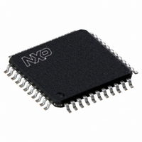
P89CV51RD2FBC,557 NXP Semiconductors, P89CV51RD2FBC,557 Datasheet - Page 16

P89CV51RD2FBC,557
Manufacturer Part Number
P89CV51RD2FBC,557
Description
IC 80C51 MCU FLASH 64K 44-TQFP
Manufacturer
NXP Semiconductors
Series
89Cr
Datasheet
1.P89CV51RB2FA512.pdf
(76 pages)
Specifications of P89CV51RD2FBC,557
Core Processor
8051
Core Size
8-Bit
Speed
40MHz
Connectivity
EBI/EMI, SPI, UART/USART
Peripherals
POR, PWM, WDT
Number Of I /o
32
Program Memory Size
64KB (64K x 8)
Program Memory Type
FLASH
Ram Size
1K x 8
Voltage - Supply (vcc/vdd)
4.5 V ~ 5.5 V
Oscillator Type
Internal
Operating Temperature
-40°C ~ 85°C
Package / Case
44-TQFP, 44-VQFP
Processor Series
P89CV5x
Core
80C51
Data Bus Width
8 bit
Data Ram Size
1 KB
Interface Type
SPI, UART
Maximum Clock Frequency
40 MHz
Number Of Programmable I/os
32
Number Of Timers
3
Operating Supply Voltage
4.5 V to 5.5 V
Maximum Operating Temperature
+ 85 C
Mounting Style
SMD/SMT
3rd Party Development Tools
PK51, CA51, A51, ULINK2
Minimum Operating Temperature
- 40 C
Cpu Family
89C
Device Core
80C51
Device Core Size
8b
Frequency (max)
40MHz
Total Internal Ram Size
1KB
# I/os (max)
32
Number Of Timers - General Purpose
3
Operating Supply Voltage (typ)
5V
Operating Supply Voltage (max)
5.5V
Operating Supply Voltage (min)
4.5V
Instruction Set Architecture
CISC
Operating Temp Range
-40C to 85C
Operating Temperature Classification
Industrial
Mounting
Surface Mount
Pin Count
44
Package Type
TQFP
Lead Free Status / RoHS Status
Lead free / RoHS Compliant
Eeprom Size
-
Data Converters
-
Lead Free Status / Rohs Status
Details
Other names
568-4257
935284103557
P89CV51RD2FBC
935284103557
P89CV51RD2FBC
Available stocks
Company
Part Number
Manufacturer
Quantity
Price
Company:
Part Number:
P89CV51RD2FBC,557
Manufacturer:
NXP Semiconductors
Quantity:
10 000
NXP Semiconductors
P89CV51RB2_RC2_RD2_3
Product data sheet
6.2.3 Reset
Table 8.
Not bit addressable; reset value 00H.
Table 9.
At initial power-up, the port pins will be in a random state until the oscillator has started
and the internal reset algorithm has weakly pulled all pins HIGH. Powering up the device
without a valid reset could cause the MCU to start executing instructions from an
indeterminate location. Such undefined states may inadvertently corrupt the code in the
flash. A system reset will not affect the on-chip RAM while the device is running, however,
the contents of the on-chip RAM during power-up are indeterminate.
When power is applied to the device, the RST pin must be held HIGH long enough for the
oscillator to start-up (usually several milliseconds for a low frequency crystal), in addition
to two machine cycles for a valid power-on reset. An example of a method to extend the
RST signal is to implement an RC circuit by connecting the RST pin to V
10 F capacitor and to V
During initial power-up the POF flag in the PCON register is set to indicate an initial
power-up condition. The POF flag will remain active until cleared by software.
Bit
Symbol
Bit
7, 6, 4
5
3
2
1
0
Fig 5.
Dual data pointer organization
AUXR1 - Auxiliary function register 1 (address A2H) bit allocation
AUXR1 - Auxiliary function register 1 (address A2H) bit description
Symbol
-
ENBOOT
GF2
0
-
DPS
7
-
DPS = 0
DPS = 1
AUXR1 / bit0
DPS
Rev. 03 — 25 August 2009
6
-
SS
DPTR0
DPTR1
Description
Reserved for future use. Should be set to 0 by user programs.
Enable BOOTROM
General purpose user-defined Flag.
This bit contains a hard-wired 0. Allows toggling of the DPS bit by
incrementing AUXR1, without interfering with other bits in the register.
Reserved for future use. Should be set to 0 by user programs.
Data Pointer Select. Chooses one of two data pointers for use by the
program. See text for details.
through an 8.2 k resistor as shown in
ENBOOT
5
DPH
83H
P89CV51RB2/RC2/RD2
4
-
DPL
82H
DPTR1
DPTR0
GF2
3
external data memory
80C51 with 1 kB RAM, SPI
2
0
002aaa518
Figure
© NXP B.V. 2009. All rights reserved.
DD
1
-
6.
through a
DPS
16 of 76
0


