P89CV51RD2FBC,557 NXP Semiconductors, P89CV51RD2FBC,557 Datasheet - Page 31

P89CV51RD2FBC,557
Manufacturer Part Number
P89CV51RD2FBC,557
Description
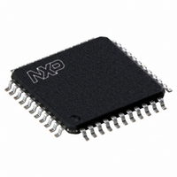
IC 80C51 MCU FLASH 64K 44-TQFP
Manufacturer
NXP Semiconductors
Series
89Cr
Datasheet
1.P89CV51RB2FA512.pdf
(76 pages)
Specifications of P89CV51RD2FBC,557
Core Processor
8051
Core Size
8-Bit
Speed
40MHz
Connectivity
EBI/EMI, SPI, UART/USART
Peripherals
POR, PWM, WDT
Number Of I /o
32
Program Memory Size
64KB (64K x 8)
Program Memory Type
FLASH
Ram Size
1K x 8
Voltage - Supply (vcc/vdd)
4.5 V ~ 5.5 V
Oscillator Type
Internal
Operating Temperature
-40°C ~ 85°C
Package / Case
44-TQFP, 44-VQFP
Processor Series
P89CV5x
Core
80C51
Data Bus Width
8 bit
Data Ram Size
1 KB
Interface Type
SPI, UART
Maximum Clock Frequency
40 MHz
Number Of Programmable I/os
32
Number Of Timers
3
Operating Supply Voltage
4.5 V to 5.5 V
Maximum Operating Temperature
+ 85 C
Mounting Style
SMD/SMT
3rd Party Development Tools
PK51, CA51, A51, ULINK2
Minimum Operating Temperature
- 40 C
Cpu Family
89C
Device Core
80C51
Device Core Size
8b
Frequency (max)
40MHz
Total Internal Ram Size
1KB
# I/os (max)
32
Number Of Timers - General Purpose
3
Operating Supply Voltage (typ)
5V
Operating Supply Voltage (max)
5.5V
Operating Supply Voltage (min)
4.5V
Instruction Set Architecture
CISC
Operating Temp Range
-40C to 85C
Operating Temperature Classification
Industrial
Mounting
Surface Mount
Pin Count
44
Package Type
TQFP
Lead Free Status / RoHS Status
Lead free / RoHS Compliant
Eeprom Size
-
Data Converters
-
Lead Free Status / Rohs Status
Details
Other names
568-4257
935284103557
P89CV51RD2FBC
935284103557
P89CV51RD2FBC
Available stocks
Company
Part Number
Manufacturer
Quantity
Price
Company:
Part Number:
P89CV51RD2FBC,557
Manufacturer:
NXP Semiconductors
Quantity:
10 000
NXP Semiconductors
P89CV51RB2_RC2_RD2_3
Product data sheet
6.5.1 Capture mode
Table 20.
Table 21.
Not bit addressable; reset value: XX00 0000B.
Table 22.
In the Capture mode there are two options which are selected by bit EXEN2 in T2CON. If
EXEN2 = 0 Timer 2 is a 16-bit timer or counter (as selected by C/T2 in T2CON) which
upon overflowing sets bit TF2, the Timer 2 overflow bit. The Capture mode is illustrated in
Figure
This bit can be used to generate an interrupt (by enabling the Timer 2 interrupt bit ET2 in
the IE register). If EXEN2 = 1, Timer 2 operates as described above, but with the added
feature that a 1-to-0 transition at external input T2EX causes the current value in the
Timer 2 registers, TL2 and TH2, to be captured into registers RCAP2L and RCAP2H,
respectively.
In addition, the transition at T2EX causes bit EXF2 in T2CON to be set, and EXF2 like
TF2 can generate an interrupt (which vectors to the same location as Timer 2 overflow
interrupt). The Timer 2 interrupt service routine can interrogate TF2 and EXF2 to
determine which event caused the interrupt.
Bit
4
3
2
1
0
Bit
Symbol
Bit
7 to 2
1
0
11.
Symbol
TCLK
EXEN2
TR2
C/T2
CP/RL2
Symbol
-
T2OE
DCEN
T2CON - Timer/Counter 2 control register (address C8H) bit description
T2MOD - Timer 2 mode control register (address C9H) bit allocation
T2MOD - Timer 2 mode control register (address C9H) bit description
7
-
Description
Transmit clock flag. When set, causes the UART to use Timer 2 overflow
pulses for its transmit clock in modes 1 and 3. TCLK = 0 causes Timer 1
overflows to be used for the transmit clock.
Timer 2 external enable flag. When set, allows a capture or reload to occur
as a result of a negative transition on T2EX if Timer 2 is not being used to
clock the serial port. EXEN2 = 0 causes Timer 2 to ignore events at T2EX.
Start/stop control for Timer 2. A logic 1 enables the timer to run.
Timer or counter select. (Timer 2)
Capture/Reload flag. When set, captures will occur on negative transitions
at T2EX if EXEN2 = 1. When cleared, auto-reloads will occur either with
Timer 2 overflows or negative transitions at T2EX when EXEN2 = 1. When
either RCLK = 1 or TCLK = 1, this bit is ignored and the timer is forced to
auto-reload on Timer 2 overflow.
Description
Reserved for future use. Should be set to 0 by user programs.
Timer 2 Output Enable bit. Used in programmable Clock-out mode only.
Down Count Enable bit. When set, this allows Timer 2 to be configured as
an up/down counter.
Rev. 03 — 25 August 2009
0 = internal timer (f
1 = external event counter (falling edge triggered; external clock’s
maximum rate = f
6
-
5
-
osc
osc
P89CV51RB2/RC2/RD2
/ 12)
/ 6)
4
-
3
-
80C51 with 1 kB RAM, SPI
2
-
© NXP B.V. 2009. All rights reserved.
T2OE
1
…continued
DCEN
31 of 76
0


