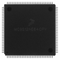
MC9S12NE64CPV Freescale Semiconductor, MC9S12NE64CPV Datasheet - Page 221

MC9S12NE64CPV
Manufacturer Part Number
MC9S12NE64CPV
Description
IC MCU 25MHZ ETHERNT/PHY 112LQFP
Manufacturer
Freescale Semiconductor
Series
HCS12r
Datasheet
1.MC9S12NE64VTU.pdf
(554 pages)
Specifications of MC9S12NE64CPV
Mfg Application Notes
MC9S12NE64 Integrated Ethernet Controller Implementing an Ethernet Interface with the MC9S12NE64 Web Server Development with MC9S12NE64 and Open TCP
Core Processor
HCS12
Core Size
16-Bit
Speed
25MHz
Connectivity
EBI/EMI, Ethernet, I²C, SCI, SPI
Peripherals
POR, PWM, WDT
Number Of I /o
70
Program Memory Size
64KB (64K x 8)
Program Memory Type
FLASH
Ram Size
8K x 8
Voltage - Supply (vcc/vdd)
2.375 V ~ 3.465 V
Data Converters
A/D 8x10b
Oscillator Type
Internal
Operating Temperature
-40°C ~ 85°C
Package / Case
112-LQFP
Data Bus Width
16 bit
Data Ram Size
8 KB
Interface Type
I2C, SCI, SPI
Maximum Clock Frequency
25 MHz
Number Of Programmable I/os
70
Number Of Timers
16 bit
Operating Supply Voltage
- 0.3 V to + 3 V
Maximum Operating Temperature
+ 105 C
Mounting Style
SMD/SMT
Minimum Operating Temperature
- 65 C
On-chip Adc
10 bit
For Use With
EVB9S12NE64E - BOARD EVAL FOR 9S12NE64DEMO9S12NE64E - DEMO BOARD FOR 9S12NE64
Lead Free Status / RoHS Status
Contains lead / RoHS non-compliant
Eeprom Size
-
Lead Free Status / Rohs Status
No RoHS Version Available
Available stocks
Company
Part Number
Manufacturer
Quantity
Price
Company:
Part Number:
MC9S12NE64CPV
Manufacturer:
RENESAS
Quantity:
21 000
Company:
Part Number:
MC9S12NE64CPV
Manufacturer:
FREESCAL
Quantity:
455
Company:
Part Number:
MC9S12NE64CPV
Manufacturer:
Freescale Semiconductor
Quantity:
10 000
Company:
Part Number:
MC9S12NE64CPVE
Manufacturer:
ST
Quantity:
445
Company:
Part Number:
MC9S12NE64CPVE
Manufacturer:
Freescale Semiconductor
Quantity:
10 000
- Current page: 221 of 554
- Download datasheet (4Mb)
7.3.2.7
This read-only register contains the sequence complete flag, overrun flags for external trigger and FIFO
mode, and the conversion counter.
Read: Anytime
Write: Anytime (No effect on (CC2, CC1, CC0))
Freescale Semiconductor
CC[2:0]
Reset
ETORF
FIFOR
Field
SCF
2–0
7
5
4
W
R
SCF
Sequence Complete Flag — This flag is set upon completion of a conversion sequence. If conversion
sequences are continuously performed (SCAN = 1), the flag is set after each one is completed. This flag is
cleared when one of the following occurs:
0 Conversion sequence not completed
1 Conversion sequence has completed
External Trigger Overrun Flag — While in edge trigger mode (ETRIGLE = 0), if additional active edges are
detected while a conversion sequence is in process the overrun flag is set. This flag is cleared when one of the
following occurs:
0 No External trigger over run error has occurred
1 External trigger over run error has occurred
FIFO Over Run Flag — This bit indicates that a result register has been written to before its associated
conversion complete flag (CCF) has been cleared. This flag is most useful when using the FIFO mode because
the flag potentially indicates that result registers are out of sync with the input channels. However, it is also
practical for non-FIFO modes, and indicates that a result register has been over written before it has been read
(i.e., the old data has been lost). This flag is cleared when one of the following occurs:
0 No over run has occurred
1 An over run condition exists
Conversion Counter — These 3 read-only bits are the binary value of the conversion counter. The conversion
counter points to the result register that will receive the result of the current conversion. E.g. CC2 = 1, CC1 = 1,
CC0 = 0 indicates that the result of the current conversion will be in ATD result register 6. If in non-FIFO mode
(FIFO = 0) the conversion counter is initialized to zero at the begin and end of the conversion sequence. If in
FIFO mode (FIFO = 1) the register counter is not initialized. The conversion counters wraps around when its
maximum value is reached.
Aborting a conversion or starting a new conversion by write to an ATDCTL register (ATDCTL5-0) clears the
conversion counter even if FIFO=1.
ATD Status Register 0 (ATDSTAT0)
0
7
A) Write “1” to SCF
B) Write to ATDCTL5 (a new conversion sequence is started)
C) If AFFC=1 and read of a result register
A) Write “1” to ETORF
B) Write to ATDCTL2, ATDCTL3 or ATDCTL4 (a conversion sequence is aborted)
C) Write to ATDCTL5 (a new conversion sequence is started)
A) Write “1” to FIFOR
B) Start a new conversion sequence (write to ATDCTL5 or external trigger)
= Unimplemented or Reserved
0
0
6
Figure 7-9. ATD Status Register 0 (ATDSTAT0)
Table 7-17. ATDSTAT0 Field Descriptions
ETORF
MC9S12NE64 Data Sheet, Rev. 1.1
0
5
FIFOR
0
4
Description
0
0
3
CC2
0
2
Memory Map and Register Definition
CC1
0
1
CC0
0
0
221
Related parts for MC9S12NE64CPV
Image
Part Number
Description
Manufacturer
Datasheet
Request
R
Part Number:
Description:
Manufacturer:
Freescale Semiconductor, Inc
Datasheet:
Part Number:
Description:
Manufacturer:
Freescale Semiconductor, Inc
Datasheet:
Part Number:
Description:
Manufacturer:
Freescale Semiconductor, Inc
Datasheet:
Part Number:
Description:
Manufacturer:
Freescale Semiconductor, Inc
Datasheet:
Part Number:
Description:
Manufacturer:
Freescale Semiconductor, Inc
Datasheet:
Part Number:
Description:
Manufacturer:
Freescale Semiconductor, Inc
Datasheet:
Part Number:
Description:
Manufacturer:
Freescale Semiconductor, Inc
Datasheet:
Part Number:
Description:
Manufacturer:
Freescale Semiconductor, Inc
Datasheet:
Part Number:
Description:
Manufacturer:
Freescale Semiconductor, Inc
Datasheet:
Part Number:
Description:
Manufacturer:
Freescale Semiconductor, Inc
Datasheet:
Part Number:
Description:
Manufacturer:
Freescale Semiconductor, Inc
Datasheet:
Part Number:
Description:
Manufacturer:
Freescale Semiconductor, Inc
Datasheet:
Part Number:
Description:
Manufacturer:
Freescale Semiconductor, Inc
Datasheet:
Part Number:
Description:
Manufacturer:
Freescale Semiconductor, Inc
Datasheet:
Part Number:
Description:
Manufacturer:
Freescale Semiconductor, Inc
Datasheet:


