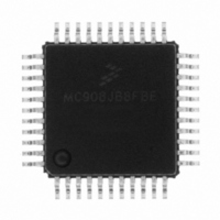
MC908JB8FBE Freescale Semiconductor, MC908JB8FBE Datasheet - Page 257

MC908JB8FBE
Manufacturer Part Number
MC908JB8FBE
Description
IC MCU 8K FLASH 3MHZ 44-QFP
Manufacturer
Freescale Semiconductor
Series
HC08r
Datasheet
1.MC908JB8JDWE.pdf
(286 pages)
Specifications of MC908JB8FBE
Core Processor
HC08
Core Size
8-Bit
Speed
3MHz
Connectivity
USB
Peripherals
LVD, POR, PWM
Number Of I /o
37
Program Memory Size
8KB (8K x 8)
Program Memory Type
FLASH
Ram Size
256 x 8
Voltage - Supply (vcc/vdd)
4 V ~ 5.5 V
Oscillator Type
Internal
Operating Temperature
0°C ~ 70°C
Package / Case
44-QFP
Processor Series
HC08JB
Core
HC08
Data Bus Width
8 bit
Data Ram Size
256 B
Interface Type
USB
Maximum Clock Frequency
3 MHz
Number Of Programmable I/os
37
Number Of Timers
2
Operating Supply Voltage
5.25 V
Maximum Operating Temperature
+ 70 C
Mounting Style
SMD/SMT
Development Tools By Supplier
FSICEBASE, DEMO908GZ60E, M68EML08GZE, KITUSBSPIDGLEVME, KITUSBSPIEVME, KIT33810EKEVME
Minimum Operating Temperature
0 C
Controller Family/series
HC08
No. Of I/o's
37
Ram Memory Size
256Byte
Cpu Speed
8MHz
No. Of Timers
1
Embedded Interface Type
SCI, SPI
Rohs Compliant
Yes
Package
44PQFP
Family Name
HC08
Maximum Speed
3 MHz
Cpu Family
HC08
Device Core Size
8b
Frequency (max)
3MHz
Total Internal Ram Size
256Byte
# I/os (max)
37
Number Of Timers - General Purpose
2
Operating Supply Voltage (typ)
5V
Operating Supply Voltage (max)
5.5V
Operating Supply Voltage (min)
4V
Instruction Set Architecture
CISC
Operating Temp Range
0C to 70C
Operating Temperature Classification
Commercial
Mounting
Surface Mount
Pin Count
44
Package Type
PQFP
Lead Free Status / RoHS Status
Lead free / RoHS Compliant
Eeprom Size
-
Data Converters
-
Lead Free Status / Rohs Status
Lead free / RoHS Compliant
Available stocks
Company
Part Number
Manufacturer
Quantity
Price
Company:
Part Number:
MC908JB8FBE
Manufacturer:
FREESCALE
Quantity:
586
Company:
Part Number:
MC908JB8FBE
Manufacturer:
Freescale Semiconductor
Quantity:
10 000
Part Number:
MC908JB8FBE
Manufacturer:
FREESCALE
Quantity:
20 000
18.7 Control Timing
18.8 Oscillator Characteristics
MC68HC908JB8•MC68HC08JB8•MC68HC08JT8 — Rev. 2.3
Freescale Semiconductor
NOTES:
NOTES:
NOTES:
Internal operating frequency
RST input pulse width low
Crystal frequency
External clock
Reference frequency
Crystal load capacitance
Crystal fixed capacitance
Crystal tuning capacitance
Feedback bias resistor
Series resistor
1. V
2. Typical values reflect average measurements at midpoint of voltage range, 25 °C only.
3. Run (operating) I
4. Wait I
5. STOP I
6. Maximum is highest voltage that POR is guaranteed.
7. If minimum V
1. V
2. Some modules may require a minimum frequency greater than dc for proper operation; see appropriate table for this infor-
3. Minimum pulse width reset is guaranteed to be recognized. It is possible for a smaller pulse width to cause a reset.
1. The USB module is designed to function at f
2. No more than 10% duty cycle deviation from 50%.
3. Consult crystal vendor data sheet.
4. Not required for high-frequency crystals.
loads. Less than 100 pF on all outputs. C
affects run I
than 100 pF on all outputs. C
as inputs; OSC2 capacitance linearly affects wait I
and D– and 15 kΩ ± 5% termination resistors on D+ and D– pins; no port pins sourcing current.
V
mation.
DD
DD
REG
= 4.0 to 5.5 Vdc, V
= 4.0 to 5.5 Vdc; V
DD
is reached.
DD
measured using external square wave clock source (f
Characteristic
measured with USB in suspend mode; OSC1 grounded; transceiver pullup resistor of 1.5 kΩ ± 5% between V
DD
REG
(3), (4)
. Measured with all modules enabled.
(1)
DD
is not reached before the internal POR reset is released, RST must be driven low externally until minimum
measured using external square wave clock source (f
(1), (2)
Characteristic
SS
SS
(3)
(3)
(3)
= 0 Vdc, T
= 0 Vdc; timing shown with respect to 20% V
(3)
(2)
L
= 20 pF on OSC2; 15 kΩ ± 5% termination resistors on D+ and D– pins; all ports configured
A
= T
(1)
L
L
to T
= 20 pF on OSC2. All ports configured as inputs. OSC2 capacitance linearly
XCLK
Symbol
Electrical Specifications
f
f
XCLK
XCLK
H
C
C
C
R
R
, unless otherwise noted.
B
S
= 6 MHz.
L
1
2
DD
Min
XCLK
dc
—
—
—
—
—
1
= 6 MHz); all inputs 0.2 V from rail; no dc loads; less
Symbol
DD
t
f
IRL
OP
XCLK
and 70% V
10 MΩ
2 × C
2 × C
Typ
—
—
—
—
= 6 MHz). All inputs 0.2 V from rail. No dc
L
L
DD
Min
125
—
, unless otherwise noted.
Max
—
—
—
—
—
Electrical Specifications
6
6
Max
—
3
Technical Data
Control Timing
MHz
MHz
Unit
MHz
Unit
ns
REG
257


