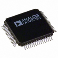
ADUC7024BSTZ62 Analog Devices Inc, ADUC7024BSTZ62 Datasheet - Page 52

ADUC7024BSTZ62
Manufacturer Part Number
ADUC7024BSTZ62
Description
IC MCU FLASH 62K ANLG I/O 64LQFP
Manufacturer
Analog Devices Inc
Series
MicroConverter® ADuC7xxxr
Specifications of ADUC7024BSTZ62
Core Size
16/32-Bit
Program Memory Size
62KB (62K x 8)
Design Resources
Sensing Low-g Acceleration Using ADXL345 Digital Accelerometer Connected to ADuC7024 (CN0133)
Core Processor
ARM7
Speed
44MHz
Connectivity
EBI/EMI, I²C, SPI, UART/USART
Peripherals
PLA, PWM, PSM, Temp Sensor, WDT
Number Of I /o
30
Program Memory Type
FLASH
Ram Size
8K x 8
Voltage - Supply (vcc/vdd)
2.7 V ~ 3.6 V
Data Converters
A/D 10x12b; D/A 2x12b
Oscillator Type
Internal
Operating Temperature
-40°C ~ 125°C
Package / Case
64-LQFP
Controller Family/series
(ARM7) ADUC
No. Of I/o's
30
Ram Memory Size
8KB
Cpu Speed
44MHz
No. Of Timers
4
Digital Ic Case Style
LQFP
Embedded Interface Type
I2C, SPI, UART
Rohs Compliant
Yes
Package
64LQFP
Device Core
ARM7TDMI
Family Name
ADuC7xxx
Maximum Speed
44 MHz
Operating Supply Voltage
3.3 V
Data Bus Width
16|32 Bit
Number Of Programmable I/os
30
Interface Type
I2C/SPI/UART
On-chip Adc
10-chx12-bit
On-chip Dac
2-chx12-bit
Number Of Timers
4
Lead Free Status / RoHS Status
Lead free / RoHS Compliant
Eeprom Size
-
Lead Free Status / RoHS Status
Lead free / RoHS Compliant, Lead free / RoHS Compliant
Available stocks
Company
Part Number
Manufacturer
Quantity
Price
Company:
Part Number:
ADUC7024BSTZ62
Manufacturer:
AD
Quantity:
261
Company:
Part Number:
ADUC7024BSTZ62
Manufacturer:
ADI
Quantity:
248
Company:
Part Number:
ADUC7024BSTZ62
Manufacturer:
Analog Devices Inc
Quantity:
10 000
Part Number:
ADUC7024BSTZ62
Manufacturer:
ADI/亚德诺
Quantity:
20 000
Company:
Part Number:
ADUC7024BSTZ62-RL
Manufacturer:
VISHAY
Quantity:
120
Company:
Part Number:
ADUC7024BSTZ62-RL
Manufacturer:
Analog Devices Inc
Quantity:
10 000
ADuC7019/20/21/22/24/25/26/27/28/29
OTHER ANALOG PERIPHERALS
DAC
The ADuC7019/20/21/22/24/25/26/27/28/29 incorporate two,
three, or four 12-bit voltage output DACs on-chip, depending on
the model. Each DAC has a rail-to-rail voltage output buffer
capable of driving 5 kΩ/100 pF.
Each DAC has three selectable ranges: 0 V to V
band gap 2.5 V reference), 0 V to DAC
DAC
The signal range is 0 V to AV
MMRs Interface
Each DAC is independently configurable through a control
register and a data register. These two registers are identical for
the four DACs. Only DAC0CON (see Table 50) and DAC0DAT
(see Table 52) are described in detail in this section.
Table 49. DACxCON Registers
Name
DAC0CON
DAC1CON
DAC2CON
DAC3CON
Table 50. DAC0CON MMR Bit Designations
Bit
7:6
5
4
3
2
1:0
REF
Name
DACCLR
DACCLK
is equivalent to an external reference for the DAC.
Address
0xFFFF0600
0xFFFF0608
0xFFFF0610
0xFFFF0618
Value
00
01
10
11
Description
Reserved.
DAC update rate. Set by user to
update the DAC using Timer1.
Cleared by user to update the DAC
using HCLK (core clock).
DAC clear bit. Set by user to enable
normal DAC operation. Cleared by
user to reset data register of the DAC
to 0.
Reserved. This bit should be left at 0.
Reserved. This bit should be left at 0.
DAC range bits.
Power-down mode. The DAC output is
in three-state.
0 V to DAC
0 V to V
0 V to AV
DD
.
Default Value
0x00
0x00
0x00
0x00
REF
DD
(2.5 V) range.
REF
range.
REF
range.
, and 0 V to AV
REF
(internal
Access
R/W
R/W
R/W
R/W
DD
.
Rev. C | Page 52 of 96
Table 51. DACxDAT Registers
Name
DAC0DAT
DAC1DAT
DAC2DAT
DAC3DAT
Table 52. DAC0DAT MMR Bit Designations
Bit
31:28
27:16
15:0
Using the DACs
The on-chip DAC architecture consists of a resistor string DAC
followed by an output buffer amplifier. The functional equivalent
is shown in Figure 53.
As illustrated in Figure 53, the reference source for each DAC is
user-selectable in software. It can be AV
0-to-AV
V to the voltage at the AV
output transfer function spans from 0 V to the voltage at the
DAC
spans from 0 V to the internal 2.5 V reference, V
The DAC output buffer amplifier features a true, rail-to-rail
output stage implementation. This means that when unloaded,
each output is capable of swinging to within less than 5 mV of
both AV
(when driving a 5 kΩ resistive load to ground) is guaranteed
through the full transfer function, except Code 0 to Code 100,
and, in 0-to-AV
REF
pin. In 0-to-V
DD
DD
mode, the DAC output transfer function spans from 0
and ground. Moreover, the DAC’s linearity specification
DAC
AV
V
Address
0xFFFF0604
0xFFFF060C
0xFFFF0614
0xFFFF061C
REF
REF
DD
DD
Description
Reserved.
12-bit data for DAC0.
Reserved.
mode only, Code 3995 to Code 4095.
REF
Figure 53. DAC Structure
mode, the DAC output transfer function
DD
R
R
R
R
R
pin. In 0-to-DAC
Default Value
0x00000000
0x00000000
0x00000000
0x00000000
DD
, V
REF
REF
, or DAC
REF
mode, the DAC
DAC0
.
Access
R/W
R/W
R/W
R/W
REF
. In


