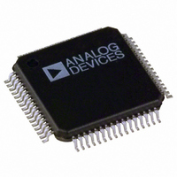
ADUC7024BSTZ62 Analog Devices Inc, ADUC7024BSTZ62 Datasheet - Page 49

ADUC7024BSTZ62
Manufacturer Part Number
ADUC7024BSTZ62
Description
IC MCU FLASH 62K ANLG I/O 64LQFP
Manufacturer
Analog Devices Inc
Series
MicroConverter® ADuC7xxxr
Specifications of ADUC7024BSTZ62
Core Size
16/32-Bit
Program Memory Size
62KB (62K x 8)
Design Resources
Sensing Low-g Acceleration Using ADXL345 Digital Accelerometer Connected to ADuC7024 (CN0133)
Core Processor
ARM7
Speed
44MHz
Connectivity
EBI/EMI, I²C, SPI, UART/USART
Peripherals
PLA, PWM, PSM, Temp Sensor, WDT
Number Of I /o
30
Program Memory Type
FLASH
Ram Size
8K x 8
Voltage - Supply (vcc/vdd)
2.7 V ~ 3.6 V
Data Converters
A/D 10x12b; D/A 2x12b
Oscillator Type
Internal
Operating Temperature
-40°C ~ 125°C
Package / Case
64-LQFP
Controller Family/series
(ARM7) ADUC
No. Of I/o's
30
Ram Memory Size
8KB
Cpu Speed
44MHz
No. Of Timers
4
Digital Ic Case Style
LQFP
Embedded Interface Type
I2C, SPI, UART
Rohs Compliant
Yes
Package
64LQFP
Device Core
ARM7TDMI
Family Name
ADuC7xxx
Maximum Speed
44 MHz
Operating Supply Voltage
3.3 V
Data Bus Width
16|32 Bit
Number Of Programmable I/os
30
Interface Type
I2C/SPI/UART
On-chip Adc
10-chx12-bit
On-chip Dac
2-chx12-bit
Number Of Timers
4
Lead Free Status / RoHS Status
Lead free / RoHS Compliant
Eeprom Size
-
Lead Free Status / RoHS Status
Lead free / RoHS Compliant, Lead free / RoHS Compliant
Available stocks
Company
Part Number
Manufacturer
Quantity
Price
Company:
Part Number:
ADUC7024BSTZ62
Manufacturer:
AD
Quantity:
261
Company:
Part Number:
ADUC7024BSTZ62
Manufacturer:
ADI
Quantity:
248
Company:
Part Number:
ADUC7024BSTZ62
Manufacturer:
Analog Devices Inc
Quantity:
10 000
Part Number:
ADUC7024BSTZ62
Manufacturer:
ADI/亚德诺
Quantity:
20 000
Company:
Part Number:
ADUC7024BSTZ62-RL
Manufacturer:
VISHAY
Quantity:
120
Company:
Part Number:
ADUC7024BSTZ62-RL
Manufacturer:
Analog Devices Inc
Quantity:
10 000
Table 35. FEECON Register
Name
FEECON
FEECON is an 8-bit command register. The commands are
described in Table 36.
Table 36. Command Codes in FEECON
Code
0x00
0x01
0x02
0x03
0x04
0x05
0x06
0x07
0x08
0x09
0x0A
0x0B
0x0C
0x0D
0x0E
0x0F
1
The FEECON register always reads 0x07 immediately after execution of any
of these commands.
1
1
1
1
1
1
1
Command
Null
Single read
Single write
Erase/write
Single verify
Single erase
Mass erase
Reserved
Reserved
Reserved
Reserved
Signature
Protect
Reserved
Reserved
Ping
Address
0xFFFFF808
Description
Idle state.
Load FEEDAT with the 16-bit data.
Indexed by FEEADR.
Write FEEDAT at the address pointed to
by FEEADR. This operation takes 50 μs.
Erase the page indexed by FEEADR and
write FEEDAT at the location pointed by
FEEADR. This operation takes approxi-
mately 24 ms.
Compare the contents of the location
pointed by FEEADR to the data in
FEEDAT. The result of the comparison is
returned in FEESTA, Bit 1.
Erase the page indexed by FEEADR.
Erase 62 kB of user space. The 2 kB of
kernel are protected. This operation
takes 2.48 sec. To prevent accidental
execution, a command sequence is
required to execute this instruction.
See the Command Sequence for
Executing a Mass Erase section.
Reserved.
Reserved.
Reserved.
Reserved.
Give a signature of the 64 kB of Flash/EE
in the 24-bit FEESIGN MMR. This
operation takes 32,778 clock cycles.
This command can run only once. The
value of FEEPRO is saved and removed
only with a mass erase (0x06) of the key.
Reserved.
Reserved.
No operation; interrupt generated.
Default Value
0x07
Access
R/W
Rev. C | Page 49 of 96
Table 37. FEEDAT Register
Name
FEEDAT
1
FEEDAT is a 16-bit data register.
Table 38. FEEADR Register
Name
FEEADR
FEEADR is another 16-bit address register.
Table 39. FEESIGN Register
Name
FEESIGN
FEESIGN is a 24-bit code signature.
Table 40. FEEPRO Register
Name
FEEPRO
FEEPRO MMR provides protection following a subsequent
reset of the MMR. It requires a software key (see Table 42).
Table 41. FEEHIDE Register
Name
FEEHIDE
FEEHIDE MMR provides immediate protection. It does not
require any software key. Note that the protection settings in
FEEHIDE are cleared by a reset (see Table 42).
Table 42. FEEPRO and FEEHIDE MMR Bit Designations
Bit
31
30:0
Command Sequence for Executing a Mass Erase
FEEDAT=0x3CFF;
FEEADR = 0xFFC3;
FEEMOD= FEEMOD|0x8;
FEECON=0x06;
ADuC7019/20/21/22/24/25/26/27/28/29
X = 0, 1, 2, or 3.
Description
Read protection. Cleared by user to protect all code.
Set by user to allow reading the code.
Write protection for Page 123 to Page 120, Page 119
to Page 116, and Page 0 to Page 3. Cleared by user to
protect the pages from writing. Set by user to allow
writing the pages.
Address
0xFFFFF80C
Address
0xFFFFF810
Address
0xFFFFF818
Address
0xFFFFF81C
Address
0xFFFFF820
//Erase key enable
//Mass erase command
Default Value
0xXXXX
Default Value
0x0000
Default Value
0xFFFFFF
Default Value
0x00000000
Default Value
0xFFFFFFFF
1
Access
R/W
Access
R/W
Access
R
Access
R/W
Access
R/W


