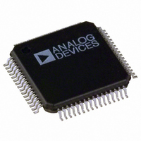
ADUC7024BSTZ62 Analog Devices Inc, ADUC7024BSTZ62 Datasheet - Page 48

ADUC7024BSTZ62
Manufacturer Part Number
ADUC7024BSTZ62
Description
IC MCU FLASH 62K ANLG I/O 64LQFP
Manufacturer
Analog Devices Inc
Series
MicroConverter® ADuC7xxxr
Specifications of ADUC7024BSTZ62
Core Size
16/32-Bit
Program Memory Size
62KB (62K x 8)
Design Resources
Sensing Low-g Acceleration Using ADXL345 Digital Accelerometer Connected to ADuC7024 (CN0133)
Core Processor
ARM7
Speed
44MHz
Connectivity
EBI/EMI, I²C, SPI, UART/USART
Peripherals
PLA, PWM, PSM, Temp Sensor, WDT
Number Of I /o
30
Program Memory Type
FLASH
Ram Size
8K x 8
Voltage - Supply (vcc/vdd)
2.7 V ~ 3.6 V
Data Converters
A/D 10x12b; D/A 2x12b
Oscillator Type
Internal
Operating Temperature
-40°C ~ 125°C
Package / Case
64-LQFP
Controller Family/series
(ARM7) ADUC
No. Of I/o's
30
Ram Memory Size
8KB
Cpu Speed
44MHz
No. Of Timers
4
Digital Ic Case Style
LQFP
Embedded Interface Type
I2C, SPI, UART
Rohs Compliant
Yes
Package
64LQFP
Device Core
ARM7TDMI
Family Name
ADuC7xxx
Maximum Speed
44 MHz
Operating Supply Voltage
3.3 V
Data Bus Width
16|32 Bit
Number Of Programmable I/os
30
Interface Type
I2C/SPI/UART
On-chip Adc
10-chx12-bit
On-chip Dac
2-chx12-bit
Number Of Timers
4
Lead Free Status / RoHS Status
Lead free / RoHS Compliant
Eeprom Size
-
Lead Free Status / RoHS Status
Lead free / RoHS Compliant, Lead free / RoHS Compliant
Available stocks
Company
Part Number
Manufacturer
Quantity
Price
Company:
Part Number:
ADUC7024BSTZ62
Manufacturer:
AD
Quantity:
261
Company:
Part Number:
ADUC7024BSTZ62
Manufacturer:
ADI
Quantity:
248
Company:
Part Number:
ADUC7024BSTZ62
Manufacturer:
Analog Devices Inc
Quantity:
10 000
Part Number:
ADUC7024BSTZ62
Manufacturer:
ADI/亚德诺
Quantity:
20 000
Company:
Part Number:
ADUC7024BSTZ62-RL
Manufacturer:
VISHAY
Quantity:
120
Company:
Part Number:
ADUC7024BSTZ62-RL
Manufacturer:
Analog Devices Inc
Quantity:
10 000
ADuC7019/20/21/22/24/25/26/27/28/29
SECURITY
The 62 kB of Flash/EE memory available to the user can be read
and write protected.
Bit 31 of the FEEPRO/FEEHIDE MMR (see Table 42) protects
the 62 kB from being read through JTAG programming mode.
The other 31 bits of this register protect writing to the flash
memory. Each bit protects four pages, that is, 2 kB. Write
protection is activated for all types of access.
Three Levels of Protection
•
•
•
Sequence to Write the Key
1.
2.
3.
4.
5.
To remove or modify the protection, the same sequence is used
with a modified value of FEEPRO. If the key chosen is the value
0xDEAD, the memory protection cannot be removed. Only a mass
erase unprotects the part, but it also erases all user code.
The sequence to write the key is illustrated in the following
example (this protects writing Page 4 to Page 7 of the Flash):
FEEPRO=0xFFFFFFFD;
FEEMOD=0x48;
FEEADR=0x1234;
FEEDAT=0x5678;
FEECON= 0x0C;
The same sequence should be followed to protect the part
permanently with FEEADR = 0xDEAD and FEEDAT = 0xDEAD.
Protection can be set and removed by writing directly into
FEEHIDE MMR. This protection does not remain after reset.
Protection can be set by writing into the FEEPRO MMR. It
takes effect only after a save protection command (0x0C)
and a reset. The FEEPRO MMR is protected by a key to
avoid direct access. The key is saved once and must be
entered again to modify FEEPRO. A mass erase sets the
key back to 0xFFFF but also erases all the user code.
Flash can be permanently protected by using the FEEPRO
MMR and a particular value of key: 0xDEADDEAD.
Entering the key again to modify the FEEPRO register is
not allowed.
Write the bit in FEEPRO corresponding to the page to be
protected.
Enable key protection by setting Bit 6 of FEEMOD (Bit 5
must equal 0).
Write a 32-bit key in FEEADR and FEEDAT.
Run the write key command 0x0C in FEECON; wait for
the read to be successful by monitoring FEESTA.
Reset the part.
//Protect pages 4 to 7
//Write key enable
//16 bit key value
//16 bit key value
// Write key command
Rev. C | Page 48 of 96
FLASH/EE CONTROL INTERFACE
Serial and JTAG programming use the Flash/EE control interface,
which includes the eight MMRs outlined in this section.
Table 31. FEESTA Register
Name
FEESTA
FEESTA is a read-only register that reflects the status of the
flash control interface as described in Table 32.
Table 32. FEESTA MMR Bit Designations
Bit
15:6
5
4
3
2
1
0
Table 33. FEEMOD Register
Name
FEEMOD
FEEMOD sets the operating mode of the flash control interface.
Table 34 shows FEEMOD MMR bit designations.
Table 34. FEEMOD MMR Bit Designations
Bit
15:9
8
7:5
4
3
2:0
Description
Reserved.
Reserved.
Reserved.
Flash interrupt status bit. Set automatically when an
interrupt occurs, that is, when a command is complete
and the Flash/EE interrupt enable bit in the FEEMOD
register is set. Cleared when reading the FEESTA register.
Flash/EE controller busy. Set automatically when the
controller is busy. Cleared automatically when the
controller is not busy.
Command fail. Set automatically when a command
completes unsuccessfully. Cleared automatically when
reading the FEESTA register.
Command pass. Set by the MicroConverter when a
command completes successfully. Cleared automatic-
ally when reading the FEESTA register.
Description
Reserved.
Reserved. This bit should always be set to 0.
Reserved. These bits should always be set to 0 except
when writing keys. See the Sequence to Write the Key
section.
Flash/EE interrupt enable. Set by user to enable the
Flash/EE interrupt. The interrupt occurs when a
command is complete. Cleared by user to disable
the Flash/EE interrupt.
Erase/write command protection. Set by user to
enable the erase and write commands. Cleared to
protect the Flash against the erase/write command.
Reserved. These bits should always be set to 0.
Address
0xFFFFF800
Address
0xFFFFF804
Default Value
0x20
Default Value
0x0000
Access
R
Access
R/W


