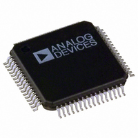
ADUC7024BSTZ62 Analog Devices Inc, ADUC7024BSTZ62 Datasheet - Page 25

ADUC7024BSTZ62
Manufacturer Part Number
ADUC7024BSTZ62
Description
IC MCU FLASH 62K ANLG I/O 64LQFP
Manufacturer
Analog Devices Inc
Series
MicroConverter® ADuC7xxxr
Specifications of ADUC7024BSTZ62
Core Size
16/32-Bit
Program Memory Size
62KB (62K x 8)
Design Resources
Sensing Low-g Acceleration Using ADXL345 Digital Accelerometer Connected to ADuC7024 (CN0133)
Core Processor
ARM7
Speed
44MHz
Connectivity
EBI/EMI, I²C, SPI, UART/USART
Peripherals
PLA, PWM, PSM, Temp Sensor, WDT
Number Of I /o
30
Program Memory Type
FLASH
Ram Size
8K x 8
Voltage - Supply (vcc/vdd)
2.7 V ~ 3.6 V
Data Converters
A/D 10x12b; D/A 2x12b
Oscillator Type
Internal
Operating Temperature
-40°C ~ 125°C
Package / Case
64-LQFP
Controller Family/series
(ARM7) ADUC
No. Of I/o's
30
Ram Memory Size
8KB
Cpu Speed
44MHz
No. Of Timers
4
Digital Ic Case Style
LQFP
Embedded Interface Type
I2C, SPI, UART
Rohs Compliant
Yes
Package
64LQFP
Device Core
ARM7TDMI
Family Name
ADuC7xxx
Maximum Speed
44 MHz
Operating Supply Voltage
3.3 V
Data Bus Width
16|32 Bit
Number Of Programmable I/os
30
Interface Type
I2C/SPI/UART
On-chip Adc
10-chx12-bit
On-chip Dac
2-chx12-bit
Number Of Timers
4
Lead Free Status / RoHS Status
Lead free / RoHS Compliant
Eeprom Size
-
Lead Free Status / RoHS Status
Lead free / RoHS Compliant, Lead free / RoHS Compliant
Available stocks
Company
Part Number
Manufacturer
Quantity
Price
Company:
Part Number:
ADUC7024BSTZ62
Manufacturer:
AD
Quantity:
261
Company:
Part Number:
ADUC7024BSTZ62
Manufacturer:
ADI
Quantity:
248
Company:
Part Number:
ADUC7024BSTZ62
Manufacturer:
Analog Devices Inc
Quantity:
10 000
Part Number:
ADUC7024BSTZ62
Manufacturer:
ADI/亚德诺
Quantity:
20 000
Company:
Part Number:
ADUC7024BSTZ62-RL
Manufacturer:
VISHAY
Quantity:
120
Company:
Part Number:
ADUC7024BSTZ62-RL
Manufacturer:
Analog Devices Inc
Quantity:
10 000
Pin No.
15
16
17
18
19
20
21
22
23
24
25
26
27
28
29
30
31
32
33
34
35
36
37
38
39
40
41
42
43
44
45
Mnemonic
TDI
P0.1/PWM2
P2.3/AE
P4.6/AD14/PLAO[14]
P4.7/AD15/PLAO[15]
BM/P0.0/CMP
P0.6/T1/MRST/PLAO[3]
TCK
TDO
P0.2/PWM2
IOGND
IOV
LV
DGND
P3.0/AD0/PWM0
P3.1/AD1/PWM0
P3.2/AD2/PWM1
P3.3/AD3/PWM1
P2.4/PWM0
P0.3/TRST/A16/ADC
P2.5/PWM0
P2.6/PWM1
RST
P3.4/AD4/PWM2
P3.5/AD5/PWM2
IRQ0/P0.4/PWM
IRQ1/P0.5/ADC
P2.0/SPM9/PLAO[5]/ CONV
P0.7/ECLK/XCLK/SPM8/PLAO[4]
XCLKO
XCLKI
DD
DD
H
L
H
L
H
/BHE
/MS1
/BLE
/MS0
/MS2
OUT
BUSY
TRIP
/PLAI[7]/MS0
H
L
H
L
H
L
/PLAI[9]
/PLAI[11]
/PLAI[13]
/PLAO[2]/MS2
/PLAI[8]
/PLAI[10]
/PLAI[12]
/PLAO[1]/MS1
BUSY
START
Description
JTAG Test Port Input, Test Data In. Debug and download access.
General-Purpose Input and Output Port 0.1/PWM Phase 2 High-Side Output/External Memory
Byte Low Enable.
General-Purpose Input and Output Port 2.3/External Memory Access Enable.
General-Purpose Input and Output Port 4.6/External Memory Interface/Programmable Logic
Array Output Element 14.
General-Purpose Input and Output Port 4.7/External Memory Interface/Programmable Logic
Array Output Element 15.
Multifunction I/O Pin. Boot Mode. The ADuC7026/ADuC7027 enter UART download mode if BM
is low at reset and execute code if BM is pulled high at reset through a 1 kΩ resistor/General-
Purpose Input and Output Port 0.0/Voltage Comparator Output/Programmable Logic Array
Input Element 7/External Memory Select 0.
Multifunction Pin, Driven Low After Reset. General-Purpose Output Port 0.6/Timer1 Input/
Power-On Reset Output/Programmable Logic Array Output Element 3.
JTAG Test Port Input, Test Clock. Debug and download access.
JTAG Test Port Output, Test Data Out. Debug and download access.
General-Purpose Input and Output Port 0.2/PWM Phase 2 Low-Side Output/External Memory
Byte High Enable.
Ground for GPIO (see Table 78). Typically connected to DGND.
3.3 V Supply for GPIO (see Table 78) and Input of the On-Chip Voltage Regulator.
2.6 V Output of the On-Chip Voltage Regulator. This output must be connected to a 0.47 μF
capacitor to DGND only.
Ground for Core Logic.
General-Purpose Input and Output Port 3.0/External Memory Interface/PWM Phase 0 High-Side
Output/Programmable Logic Array Input Element 8.
General-Purpose Input and Output Port 3.1/External Memory Interface/PWM Phase 0 Low-Side
Output/Programmable Logic Array Input Element 9.
General-Purpose Input and Output Port 3.2/External Memory Interface/PWM Phase 1 High-Side
Output/Programmable Logic Array Input Element 10.
General-Purpose Input and Output Port 3.3/External Memory Interface/PWM Phase 1 Low-Side
Output/Programmable Logic Array Input Element 11.
General-Purpose Input and Output Port 2.4/PWM Phase 0 High-Side Output/External Memory
Select 0.
General-Purpose Input and Output Port 0.3/JTAG Test Port Input, Test Reset/ADC
General-Purpose Input and Output Port 2.5/PWM Phase 0 Low-Side Output/External Memory
Select 1.
General-Purpose Input and Output Port 2.6/PWM Phase 1 High-Side Output/External Memory
Select 2.
Reset Input, Active Low.
General-Purpose Input and Output Port 3.4/External Memory Interface/PWM Phase 2 High-Side
Output/Programmable Logic Array Input 12.
General-Purpose Input and Output Port 3.5/External Memory Interface/PWM Phase 2 Low-Side
Output/Programmable Logic Array Input Element 13.
Multifunction I/O Pin. External Interrupt Request 0, Active High/General-Purpose Input and
Output Port 0.4/PWM Trip External Input/Programmable Logic Array Output Element 1/
External Memory Select 1.
Multifunction I/O Pin. External Interrupt Request 1, Active High/General-Purpose Input and
Output Port 0.5/ADC
Memory Select 2.
Serial Port Multiplexed. General-Purpose Input and Output Port 2.0/UART/Programmable Logic
Array Output Element 5/Start Conversion Input Signal for ADC.
Serial Port Multiplexed. General-Purpose Input and Output Port 0.7/Output for External Clock
Signal/Input to the Internal Clock Generator Circuits/UART/Programmable Logic Array Output
Element 4.
Output from the Crystal Oscillator Inverter.
Input to the Crystal Oscillator Inverter and Input to the Internal Clock Generator Circuits.
Rev. C | Page 25 of 96
BUSY
Signal Output/Programmable Logic Array Output Element 2/External
ADuC7019/20/21/22/24/25/26/27/28/29
BUSY
Signal Output.


