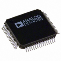
ADUC7024BSTZ62 Analog Devices Inc, ADUC7024BSTZ62 Datasheet - Page 42

ADUC7024BSTZ62
Manufacturer Part Number
ADUC7024BSTZ62
Description
IC MCU FLASH 62K ANLG I/O 64LQFP
Manufacturer
Analog Devices Inc
Series
MicroConverter® ADuC7xxxr
Specifications of ADUC7024BSTZ62
Core Size
16/32-Bit
Program Memory Size
62KB (62K x 8)
Design Resources
Sensing Low-g Acceleration Using ADXL345 Digital Accelerometer Connected to ADuC7024 (CN0133)
Core Processor
ARM7
Speed
44MHz
Connectivity
EBI/EMI, I²C, SPI, UART/USART
Peripherals
PLA, PWM, PSM, Temp Sensor, WDT
Number Of I /o
30
Program Memory Type
FLASH
Ram Size
8K x 8
Voltage - Supply (vcc/vdd)
2.7 V ~ 3.6 V
Data Converters
A/D 10x12b; D/A 2x12b
Oscillator Type
Internal
Operating Temperature
-40°C ~ 125°C
Package / Case
64-LQFP
Controller Family/series
(ARM7) ADUC
No. Of I/o's
30
Ram Memory Size
8KB
Cpu Speed
44MHz
No. Of Timers
4
Digital Ic Case Style
LQFP
Embedded Interface Type
I2C, SPI, UART
Rohs Compliant
Yes
Package
64LQFP
Device Core
ARM7TDMI
Family Name
ADuC7xxx
Maximum Speed
44 MHz
Operating Supply Voltage
3.3 V
Data Bus Width
16|32 Bit
Number Of Programmable I/os
30
Interface Type
I2C/SPI/UART
On-chip Adc
10-chx12-bit
On-chip Dac
2-chx12-bit
Number Of Timers
4
Lead Free Status / RoHS Status
Lead free / RoHS Compliant
Eeprom Size
-
Lead Free Status / RoHS Status
Lead free / RoHS Compliant, Lead free / RoHS Compliant
Available stocks
Company
Part Number
Manufacturer
Quantity
Price
Company:
Part Number:
ADUC7024BSTZ62
Manufacturer:
AD
Quantity:
261
Company:
Part Number:
ADUC7024BSTZ62
Manufacturer:
ADI
Quantity:
248
Company:
Part Number:
ADUC7024BSTZ62
Manufacturer:
Analog Devices Inc
Quantity:
10 000
Part Number:
ADUC7024BSTZ62
Manufacturer:
ADI/亚德诺
Quantity:
20 000
Company:
Part Number:
ADUC7024BSTZ62-RL
Manufacturer:
VISHAY
Quantity:
120
Company:
Part Number:
ADUC7024BSTZ62-RL
Manufacturer:
Analog Devices Inc
Quantity:
10 000
ADuC7019/20/21/22/24/25/26/27/28/29
TYPICAL OPERATION
Once configured via the ADC control and channel selection
registers, the ADC converts the analog input and provides a
12-bit result in the ADC data register.
The top four bits are the sign bits. The 12-bit result is placed
from Bit 16 to Bit 27, as shown in Figure 41. Again, it should be
noted that, in fully differential mode, the result is represented in
twos complement format. In pseudo differential and single-
ended modes, the result is represented in straight binary format.
The same format is used in DACxDAT, simplifying the software.
Current Consumption
The ADC in standby mode, that is, powered up but not
converting, typically consumes 640 μA. The internal reference
adds 140 μA. During conversion, the extra current is 0.3 μA
multiplied by the sampling frequency (in kilohertz (kHz)).
Figure 33 shows the current consumption vs. the sampling
frequency of the ADC.
Timing
Figure 42 gives details of the ADC timing. Users control the
ADC clock speed and the number of acquisition clocks in the
ADCCON MMR. By default, the acquisition time is eight clocks
and the clock divider is 2. The number of extra clocks (such as
bit trial or write) is set to 19, which gives a sampling rate of 774
kSPS. For conversion on the temperature sensor, the ADC
acquisition time is automatically set to 16 clocks, and the ADC
clock divider is set to 32. When using multiple channels,
including the temperature sensor, the timing settings revert to
the user-defined settings after reading the temperature sensor
channel.
31
SIGN BITS
27
Figure 41. ADC Result Format
12-BIT ADC RESULT
16 15
Rev. C | Page 42 of 96
0
ADC CLOCK
ADuC7019
The ADuC7019 is identical to the ADuC7020 except for one
buffered ADC channel, ADC3, and it has only three DACs. The
output buffer of the fourth DAC is internally connected to the
ADC3 channel as shown in Figure 43.
Note that the DAC3 output pin must be connected to a 10 nF
capacitor to AGND. This channel should be used to measure dc
voltages only. ADC calibration may be necessary on this channel.
MMRS INTERFACE
The ADC is controlled and configured via the eight MMRs
described in this section.
Table 17. ADCCON Register
Name
ADCCON
ADCCON is an ADC control register that allows the programmer
to enable the ADC peripheral, select the mode of operation of
the ADC (in single-ended mode, pseudo differential mode, or
fully differential mode), and select the conversion type. This
MMR is described in Table 18.
CONV
ADC
ADCDAT
START
BUSY
ADC3
Address
0xFFFF0500
MUX
ADC15
Figure 43. ADC3 Buffered Input
Figure 42. ADC Timing
ACQ
12-BIT ADC
1MSPS
BIT TRIAL
ADCSTA = 0
Default Value
0x0600
12-BIT
ADuC7019
DAC
WRITE
ADC INTERRUPT
DATA
DAC3
ADCSTA = 1
Access
R/W


