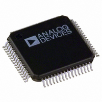
ADUC7024BSTZ62 Analog Devices Inc, ADUC7024BSTZ62 Datasheet - Page 44

ADUC7024BSTZ62
Manufacturer Part Number
ADUC7024BSTZ62
Description
IC MCU FLASH 62K ANLG I/O 64LQFP
Manufacturer
Analog Devices Inc
Series
MicroConverter® ADuC7xxxr
Specifications of ADUC7024BSTZ62
Core Size
16/32-Bit
Program Memory Size
62KB (62K x 8)
Design Resources
Sensing Low-g Acceleration Using ADXL345 Digital Accelerometer Connected to ADuC7024 (CN0133)
Core Processor
ARM7
Speed
44MHz
Connectivity
EBI/EMI, I²C, SPI, UART/USART
Peripherals
PLA, PWM, PSM, Temp Sensor, WDT
Number Of I /o
30
Program Memory Type
FLASH
Ram Size
8K x 8
Voltage - Supply (vcc/vdd)
2.7 V ~ 3.6 V
Data Converters
A/D 10x12b; D/A 2x12b
Oscillator Type
Internal
Operating Temperature
-40°C ~ 125°C
Package / Case
64-LQFP
Controller Family/series
(ARM7) ADUC
No. Of I/o's
30
Ram Memory Size
8KB
Cpu Speed
44MHz
No. Of Timers
4
Digital Ic Case Style
LQFP
Embedded Interface Type
I2C, SPI, UART
Rohs Compliant
Yes
Package
64LQFP
Device Core
ARM7TDMI
Family Name
ADuC7xxx
Maximum Speed
44 MHz
Operating Supply Voltage
3.3 V
Data Bus Width
16|32 Bit
Number Of Programmable I/os
30
Interface Type
I2C/SPI/UART
On-chip Adc
10-chx12-bit
On-chip Dac
2-chx12-bit
Number Of Timers
4
Lead Free Status / RoHS Status
Lead free / RoHS Compliant
Eeprom Size
-
Lead Free Status / RoHS Status
Lead free / RoHS Compliant, Lead free / RoHS Compliant
Available stocks
Company
Part Number
Manufacturer
Quantity
Price
Company:
Part Number:
ADUC7024BSTZ62
Manufacturer:
AD
Quantity:
261
Company:
Part Number:
ADUC7024BSTZ62
Manufacturer:
ADI
Quantity:
248
Company:
Part Number:
ADUC7024BSTZ62
Manufacturer:
Analog Devices Inc
Quantity:
10 000
Part Number:
ADUC7024BSTZ62
Manufacturer:
ADI/亚德诺
Quantity:
20 000
Company:
Part Number:
ADUC7024BSTZ62-RL
Manufacturer:
VISHAY
Quantity:
120
Company:
Part Number:
ADUC7024BSTZ62-RL
Manufacturer:
Analog Devices Inc
Quantity:
10 000
ADuC7019/20/21/22/24/25/26/27/28/29
Table 22. ADCCN MMR Bit Designation
Bit
7:5
4:0
Table 23. ADCSTA Register
Name
ADCSTA
ADCSTA is an ADC status register that indicates when an ADC
conversion result is ready. The ADCSTA register contains only
one bit, ADCReady (Bit 0), representing the status of the ADC.
This bit is set at the end of an ADC conversion, generating an
ADC interrupt. It is cleared automatically by reading the
ADCDAT MMR. When the ADC is performing a conversion,
the status of the ADC can be read externally via the ADC
pin. This pin is high during a conversion. When the conversion
is finished, ADC
available on P0.5 (see the General-Purpose Input/Output
section) if enabled in the ADCCON register.
Table 24. ADCDAT Register
Name
ADCDAT
ADCDAT is an ADC data result register. It holds the 12-bit
ADC result as shown in Figure 41.
Table 25. ADCRST Register
Name
ADCRST
ADCRST resets the digital interface of the ADC. Writing any value
to this register resets all the ADC registers to their default values.
Table 26. ADCGN Register
Name
ADCGN
ADCGN is a 10-bit gain calibration register.
Value
00000
00001
00010
00011
00100
00101
00110
00111
01000
01001
01010
01011
01100
01101
01110
01111
10000
Others
Address
0xFFFF050C
Address
0xFFFF0510
Address
0xFFFF0514
Address
0xFFFF0530
BUSY
Description
Reserved.
Negative channel selection bits.
ADC0.
ADC1.
ADC2.
ADC3.
ADC4.
ADC5.
ADC6.
ADC7.
ADC8.
ADC9.
ADC10.
ADC11.
DAC0/ADC12.
DAC1/ADC13.
DAC2/ADC14.
DAC3/ADC15.
Internal reference (self-diagnostic feature).
Reserved.
goes back low. This information can be
Default Value
0x00
Default Value
0x00000000
Default Value
0x00
Default Value
0x0200
Access
R
Access
R
Access
R/W
Access
R/W
BUSY
Rev. C | Page 44 of 96
Table 27. ADCOF Register
Name
ADCOF
ADCOF is a 10-bit offset calibration register.
CONVERTER OPERATION
The ADC incorporates a successive approximation (SAR)
architecture involving a charge-sampled input stage. This
architecture can operate in three modes: differential, pseudo
differential, and single-ended.
Differential Mode
The ADuC7019/20/21/22/24/25/26/27/28/29 each contain a
successive approximation ADC based on two capacitive DACs.
Figure 44 and Figure 45 show simplified schematics of the ADC
in acquisition and conversion phase, respectively. The ADC
comprises control logic, a SAR, and two capacitive DACs. In
Figure 44 (the acquisition phase), SW3 is closed and SW1 and
SW2 are in Position A. The comparator is held in a balanced
condition, and the sampling capacitor arrays acquire the
differential signal on the input.
AIN11
When the ADC starts a conversion, as shown in Figure 45, SW3
opens, and then SW1 and SW2 move to Position B. This causes
the comparator to become unbalanced. Both inputs are discon-
nected once the conversion begins. The control logic and the
charge redistribution DACs are used to add and subtract fixed
amounts of charge from the sampling capacitor arrays to bring
the comparator back into a balanced condition. When the
comparator is rebalanced, the conversion is complete. The
control logic generates the ADC output code. The output
impedances of the sources driving the V
voltage pins must be matched; otherwise, the two inputs have
different settling times, resulting in errors.
AIN11
AIN0
AIN0
MUX
MUX
CHANNEL+
CHANNEL–
CHANNEL+
CHANNEL–
Address
0xFFFF0534
Figure 44. ADC Acquisition Phase
Figure 45. ADC Conversion Phase
B
A
A
B
B
A
A
B
V
V
REF
REF
SW1
SW2
SW1
SW2
C
C
C
C
S
S
S
S
Default Value
0x0200
SW3
SW3
COMPARATOR
COMPARATOR
IN+
and V
IN–
CAPACITIVE
CAPACITIVE
CAPACITIVE
CAPACITIVE
input
CONTROL
CONTROL
DAC
LOGIC
DAC
DAC
LOGIC
DAC
Access
R/W


