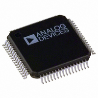
ADUC7024BSTZ62 Analog Devices Inc, ADUC7024BSTZ62 Datasheet - Page 45

ADUC7024BSTZ62
Manufacturer Part Number
ADUC7024BSTZ62
Description
IC MCU FLASH 62K ANLG I/O 64LQFP
Manufacturer
Analog Devices Inc
Series
MicroConverter® ADuC7xxxr
Specifications of ADUC7024BSTZ62
Core Size
16/32-Bit
Program Memory Size
62KB (62K x 8)
Design Resources
Sensing Low-g Acceleration Using ADXL345 Digital Accelerometer Connected to ADuC7024 (CN0133)
Core Processor
ARM7
Speed
44MHz
Connectivity
EBI/EMI, I²C, SPI, UART/USART
Peripherals
PLA, PWM, PSM, Temp Sensor, WDT
Number Of I /o
30
Program Memory Type
FLASH
Ram Size
8K x 8
Voltage - Supply (vcc/vdd)
2.7 V ~ 3.6 V
Data Converters
A/D 10x12b; D/A 2x12b
Oscillator Type
Internal
Operating Temperature
-40°C ~ 125°C
Package / Case
64-LQFP
Controller Family/series
(ARM7) ADUC
No. Of I/o's
30
Ram Memory Size
8KB
Cpu Speed
44MHz
No. Of Timers
4
Digital Ic Case Style
LQFP
Embedded Interface Type
I2C, SPI, UART
Rohs Compliant
Yes
Package
64LQFP
Device Core
ARM7TDMI
Family Name
ADuC7xxx
Maximum Speed
44 MHz
Operating Supply Voltage
3.3 V
Data Bus Width
16|32 Bit
Number Of Programmable I/os
30
Interface Type
I2C/SPI/UART
On-chip Adc
10-chx12-bit
On-chip Dac
2-chx12-bit
Number Of Timers
4
Lead Free Status / RoHS Status
Lead free / RoHS Compliant
Eeprom Size
-
Lead Free Status / RoHS Status
Lead free / RoHS Compliant, Lead free / RoHS Compliant
Available stocks
Company
Part Number
Manufacturer
Quantity
Price
Company:
Part Number:
ADUC7024BSTZ62
Manufacturer:
AD
Quantity:
261
Company:
Part Number:
ADUC7024BSTZ62
Manufacturer:
ADI
Quantity:
248
Company:
Part Number:
ADUC7024BSTZ62
Manufacturer:
Analog Devices Inc
Quantity:
10 000
Part Number:
ADUC7024BSTZ62
Manufacturer:
ADI/亚德诺
Quantity:
20 000
Company:
Part Number:
ADUC7024BSTZ62-RL
Manufacturer:
VISHAY
Quantity:
120
Company:
Part Number:
ADUC7024BSTZ62-RL
Manufacturer:
Analog Devices Inc
Quantity:
10 000
Pseudo Differential Mode
In pseudo differential mode, Channel− is linked to the V
of the ADuC7019/20/21/22/24/25/26/27/28/29. SW2 switches
between A (Channel−) and B (V
connected to ground or a low voltage. The input signal on V
can then vary from V
chosen so that V
AIN11
Single-Ended Mode
In single-ended mode, SW2 is always connected internally to
ground. The V
V
AIN11
Analog Input Structure
Figure 48 shows the equivalent circuit of the analog input structure
of the ADC. The four diodes provide ESD protection for the analog
inputs. Care must be taken to ensure that the analog input
signals never exceed the supply rails by more than 300 mV;
exceeding 300 mV causes these diodes to become forward-
biased and start conducting into the substrate. These diodes can
conduct up to 10 mA without causing irreversible damage to
the part.
The C1 capacitors in Figure 48 are typically 4 pF and can be
primarily attributed to pin capacitance. The resistors are
lumped components made up of the on resistance of the
switches. The value of these resistors is typically about 100 Ω.
The C2 capacitors are the ADC’s sampling capacitors and
typically have a capacitance of 16 pF.
AIN0
AIN0
V
IN+
IN–
is 0 V to V
MUX
MUX
CHANNEL+
CHANNEL–
CHANNEL+
Figure 46. ADC in Pseudo Differential Mode
IN−
REF
REF
Figure 47. ADC in Single-Ended Mode
pin can be floating. The input signal range on
CHANNEL–
.
+ V
B
A
A
B
B
A
IN−
V
REF
SW1
SW2
SW1
IN−
to V
does not exceed AV
C
C
C
C
REF
S
S
S
S
+ V
REF
). The V
IN−
SW3
SW3
. Note that V
COMPARATOR
COMPARATOR
IN−
pin must be
DD
.
IN−
CAPACITIVE
CAPACITIVE
CAPACITIVE
CAPACITIVE
CONTROL
CONTROL
must be
DAC
DAC
DAC
DAC
LOGIC
LOGIC
IN−
pin
IN+
Rev. C | Page 45 of 96
For ac applications, removing high frequency components from
the analog input signal is recommended by using an RC low-
pass filter on the relevant analog input pins. In applications
where harmonic distortion and signal-to-noise ratio are critical,
the analog input should be driven from a low impedance
source. Large source impedances significantly affect the ac
performance of the ADC. This can necessitate the use of an
input buffer amplifier. The choice of the op amp is a function of
the particular application. Figure 49 and Figure 50 give an
example of an ADC front end.
When no amplifier is used to drive the analog input, the source
impedance should be limited to values lower than 1 kΩ. The
maximum source impedance depends on the amount of total
harmonic distortion (THD) that can be tolerated. The THD
increases as the source impedance increases and the performance
degrades.
DRIVING THE ANALOG INPUTS
Internal or external references can be used for the ADC. In
the differential mode of operation, there are restrictions on the
common-mode input signal (V
the reference value and supply voltage used to ensure that the
signal remains within the supply rails. Table 28 gives some
calculated V
Figure 48. Equivalent Analog Input Circuit Conversion Phase: Switches Open,
ADuC7019/20/21/22/24/25/26/27/28/29
Figure 49. Buffering Single-Ended/Pseudo Differential Input
CM
V
REF
minimum and V
Figure 50. Buffering Differential Inputs
C1
C1
Track Phase: Switches Closed
AV
AV
10Ω
DD
DD
0.01µF
D
D
D
D
CM
CM
), which is dependent upon
maximum values.
ADuC7019/
ADuC702x
ADC0
ADC1
R1 C2
R1 C2
ADuC7019/
ADuC702x
ADC0


