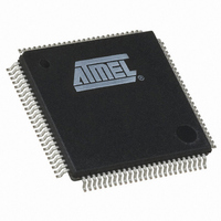
AT91SAM7A3-AU Atmel, AT91SAM7A3-AU Datasheet - Page 84

AT91SAM7A3-AU
Manufacturer Part Number
AT91SAM7A3-AU
Description
IC ARM7 MCU FLASH 256K 100LQFP
Manufacturer
Atmel
Series
AT91SAMr
Specifications of AT91SAM7A3-AU
Core Processor
ARM7
Core Size
16/32-Bit
Speed
60MHz
Connectivity
CAN, I²C, MMC, SPI, SSC, UART/USART
Peripherals
POR, PWM, WDT
Number Of I /o
62
Program Memory Size
256KB (256K x 8)
Program Memory Type
FLASH
Ram Size
32K x 8
Voltage - Supply (vcc/vdd)
1.65 V ~ 1.95 V
Data Converters
A/D 8x10b
Oscillator Type
Internal
Operating Temperature
-40°C ~ 85°C
Package / Case
100-LQFP
Controller Family/series
AT91SAM7xx
No. Of I/o's
62
Ram Memory Size
32KB
Cpu Speed
60MHz
No. Of Timers
3
Rohs Compliant
Yes
Package
100LQFP
Device Core
ARM7TDMI
Family Name
91S
Maximum Speed
60 MHz
Operating Supply Voltage
3.3 V
Data Bus Width
32 Bit
Number Of Programmable I/os
62
Interface Type
CAN/SPI/I2S/TWI/USART/USB
On-chip Adc
2(8-chx10-bit)
Number Of Timers
3
Processor Series
AT91SAMx
Core
ARM7TDMI
Data Ram Size
32 KB
Maximum Clock Frequency
60 MHz
Maximum Operating Temperature
+ 85 C
Mounting Style
SMD/SMT
3rd Party Development Tools
JTRACE-ARM-2M, MDK-ARM, RL-ARM, ULINK2
Development Tools By Supplier
AT91SAM-ICE, AT91-ISP, AT91SAM7A3-EK
Minimum Operating Temperature
- 40 C
Cpu Family
91S
Device Core Size
32b
Frequency (max)
60MHz
Total Internal Ram Size
32KB
# I/os (max)
62
Number Of Timers - General Purpose
3
Operating Supply Voltage (typ)
3.3V
Operating Supply Voltage (max)
3.6V
Operating Supply Voltage (min)
3V
Instruction Set Architecture
RISC
Operating Temp Range
-40C to 85C
Operating Temperature Classification
Industrial
Mounting
Surface Mount
Pin Count
100
Package Type
LQFP
For Use With
AT91SAM-ICE - EMULATOR FOR AT91 ARM7/ARM9AT91SAM7A3-EK - KIT EVAL FOR AT91SAM7A3
Lead Free Status / RoHS Status
Lead free / RoHS Compliant
Eeprom Size
-
Lead Free Status / Rohs Status
Details
Available stocks
Company
Part Number
Manufacturer
Quantity
Price
Company:
Part Number:
AT91SAM7A3-AU
Manufacturer:
MXIC
Quantity:
1 001
Company:
Part Number:
AT91SAM7A3-AU
Manufacturer:
Atmel
Quantity:
730
- Current page: 84 of 594
- Download datasheet (7Mb)
18.3
18.4
18.4.1
18.5
84
I/O Lines Description
Product Dependencies
Functional Description
AT91SAM7A3 Preliminary
Power Management
Table 18-1.
The Shutdown Controller is continuously clocked by Slow Clock. The Power Management
Controller has no effect on the behavior of the Shutdown Controller.
The Shutdown Controller manages the main power supply. To do so, it is supplied with
VDDBU and manages wake-up input pins and one output pin, SHDW.
A typical application connects the pin SHDW to the shutdown input of the DC/DC Converter
providing the main power supplies of the system, and especially VDD1V8 and/or VDD3V3.
The wake-up inputs (WKUP0, WKUP1, FWKUP) connect to any push-buttons or signal that
wake up the system.
The software is able to control the pin SHDW by writing the Shutdown Control Register
(SHDW_CR) with the bit SHDW at 1. This register is password-protected and so the value
written should contain the correct key for the command to be taken into account. As a result,
the system should be powered down.
A level change on WKUP0 or WKUP1 is used as wake-up. Wake-up is configured in the Shut-
down Mode Register (SHDW_MR). The transition detector can be programmed to detect
either a positive or negative transition or any level change on WKUP0 and WKUP1. The
detection can also be disabled. Programming is performed by defining WKMODE0 and
WKMODE1.
Moreover, a debouncing circuit can be programmed for WKUP0 or WKUP1. The debouncing
circuit filters pulses on WKUP0 or WKUP1 shorter than the programmed number of 16 SLCK
cycles in CPTWK0 or CPTWK1 of the SHDW_MR register. If the programmed level change is
detected on a pin, a counter starts. When the counter reaches the value programmed in the
corresponding field, CPTWK0 or CPTWK1, the SHDW pin is released. If a new input change
is detected before the counter reaches the corresponding value, the counter is stopped and
cleared. WAKEUP0 and/or WAKEUP1 of the Status Register (SHDW_SR) reports the detec-
tion of the programmed events on WKUP0 or WKUP1, with a reset after the read of
SHDW_SR.
The Shutdown Controller can be programmed so as to activate the wake-up using the RTT
alarm (the detection of the rising edge of the RTT alarm is synchronized with SLCK). This is
done by writing the SHDW_MR register using the RTTWKEN fields. When enabled, the detec-
tion of the RTT alarm is reported in the RTTWK bit of the SHDW_SR Status register. It is reset
Name
FWKUP
WKUP0
WKUP1
SHDW
I/O Lines Description
Description
Force Wake Up input for the Shutdown Controller
Wake-up 0 input
Wake-up 1input
Shutdown output
6042E–ATARM–14-Dec-06
Type
Input
Input
Input
Output
Related parts for AT91SAM7A3-AU
Image
Part Number
Description
Manufacturer
Datasheet
Request
R

Part Number:
Description:
MCU ARM9 64K SRAM 144-LFBGA
Manufacturer:
Atmel
Datasheet:

Part Number:
Description:
IC ARM9 MPU 217-LFBGA
Manufacturer:
Atmel
Datasheet:

Part Number:
Description:
MCU ARM9 ULTRA LOW PWR 217-LFBGA
Manufacturer:
Atmel
Datasheet:

Part Number:
Description:
MCU ARM9 324-TFBGA
Manufacturer:
Atmel
Datasheet:

Part Number:
Description:
IC MCU ARM9 SAMPLING 217CBGA
Manufacturer:
Atmel
Datasheet:

Part Number:
Description:
IC ARM9 MCU 217-LFBGA
Manufacturer:
Atmel
Datasheet:

Part Number:
Description:
IC ARM9 MCU 208-PQFP
Manufacturer:
Atmel
Datasheet:

Part Number:
Description:
MCU ARM 512K HS FLASH 100-LQFP
Manufacturer:
Atmel
Datasheet:

Part Number:
Description:
MCU ARM 512K HS FLASH 100-TFBGA
Manufacturer:
Atmel
Datasheet:

Part Number:
Description:
IC ARM9 MCU 200 MHZ 324-TFBGA
Manufacturer:
Atmel
Datasheet:

Part Number:
Description:
IC ARM MCU 16BIT 128K 256BGA
Manufacturer:
Atmel
Datasheet:

Part Number:
Description:
IC ARM7 MCU 32BIT 128K 64LQFP
Manufacturer:
Atmel
Datasheet:

Part Number:
Description:
IC ARM7 MCU FLASH 256K 128-LQFP
Manufacturer:
Atmel
Datasheet:

Part Number:
Description:
IC ARM7 MCU FLASH 512K 128-LQFP
Manufacturer:
Atmel
Datasheet:

Part Number:
Description:
IC ARM9 MPU 217-LFBGA
Manufacturer:
Atmel
Datasheet:


