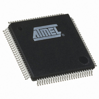
AT91SAM7A3-AU Atmel, AT91SAM7A3-AU Datasheet - Page 107

AT91SAM7A3-AU
Manufacturer Part Number
AT91SAM7A3-AU
Description
IC ARM7 MCU FLASH 256K 100LQFP
Manufacturer
Atmel
Series
AT91SAMr
Specifications of AT91SAM7A3-AU
Core Processor
ARM7
Core Size
16/32-Bit
Speed
60MHz
Connectivity
CAN, I²C, MMC, SPI, SSC, UART/USART
Peripherals
POR, PWM, WDT
Number Of I /o
62
Program Memory Size
256KB (256K x 8)
Program Memory Type
FLASH
Ram Size
32K x 8
Voltage - Supply (vcc/vdd)
1.65 V ~ 1.95 V
Data Converters
A/D 8x10b
Oscillator Type
Internal
Operating Temperature
-40°C ~ 85°C
Package / Case
100-LQFP
Controller Family/series
AT91SAM7xx
No. Of I/o's
62
Ram Memory Size
32KB
Cpu Speed
60MHz
No. Of Timers
3
Rohs Compliant
Yes
Package
100LQFP
Device Core
ARM7TDMI
Family Name
91S
Maximum Speed
60 MHz
Operating Supply Voltage
3.3 V
Data Bus Width
32 Bit
Number Of Programmable I/os
62
Interface Type
CAN/SPI/I2S/TWI/USART/USB
On-chip Adc
2(8-chx10-bit)
Number Of Timers
3
Processor Series
AT91SAMx
Core
ARM7TDMI
Data Ram Size
32 KB
Maximum Clock Frequency
60 MHz
Maximum Operating Temperature
+ 85 C
Mounting Style
SMD/SMT
3rd Party Development Tools
JTRACE-ARM-2M, MDK-ARM, RL-ARM, ULINK2
Development Tools By Supplier
AT91SAM-ICE, AT91-ISP, AT91SAM7A3-EK
Minimum Operating Temperature
- 40 C
Cpu Family
91S
Device Core Size
32b
Frequency (max)
60MHz
Total Internal Ram Size
32KB
# I/os (max)
62
Number Of Timers - General Purpose
3
Operating Supply Voltage (typ)
3.3V
Operating Supply Voltage (max)
3.6V
Operating Supply Voltage (min)
3V
Instruction Set Architecture
RISC
Operating Temp Range
-40C to 85C
Operating Temperature Classification
Industrial
Mounting
Surface Mount
Pin Count
100
Package Type
LQFP
For Use With
AT91SAM-ICE - EMULATOR FOR AT91 ARM7/ARM9AT91SAM7A3-EK - KIT EVAL FOR AT91SAM7A3
Lead Free Status / RoHS Status
Lead free / RoHS Compliant
Eeprom Size
-
Lead Free Status / Rohs Status
Details
Available stocks
Company
Part Number
Manufacturer
Quantity
Price
Company:
Part Number:
AT91SAM7A3-AU
Manufacturer:
MXIC
Quantity:
1 001
Company:
Part Number:
AT91SAM7A3-AU
Manufacturer:
Atmel
Quantity:
730
- Current page: 107 of 594
- Download datasheet (7Mb)
20.2.4.3
20.2.4.4
20.2.4.5
6042E–ATARM–14-Dec-06
Lock Protection
Write Page and Lock
Erase All Flash
The Clear Lock Bit command programs the lock bit to 1; the corresponding bit LOCKSx in
MC_FSR reads 0. The Set Lock Bit command programs the lock bit to 0; the corresponding bit
LOCKSx in MC_FSR reads 1.
When the Set Lock Bit or Clear Lock Bit command is triggered, the programming or erasing
operation of the lock bit is performed. When it completes, the bit EOL is set.
No access to the Flash is permitted when a Set Lock Bit or Clear Lock Bit command is
performed.
A programming error, where a bad keyword and/or an invalid command have been written in
the MC_FCR register, may be detected in the MC_FSR register after a programming
sequence.
Figure 20-7. State of the EOL Bit in MC_FSR
When a programming command is performed with PAGEN defining a locked lock region, the
bit LOCKE in MC_FSR rises. If the bit LOCKE has been written at 1 in MC_FMR, the interrupt
line rises. Reading MC_FSR automatically clears the bit LOCKE in MC_FSR and thus deacti-
vates the interrupt line.
The user can perform consecutively the programming of the page and the lock of the lock
region (Write Page and Lock Command (WPL) in the FCMD field of the Flash Command
Register MC_FCR), both defined by PAGEN.
Only one or both end of programming or end of lock interrupts may be enabled to trigger an
interrupt when the operations completes.
The entire memory can be erased if the Erase All Command (EA) in the Flash Command
Register MC_FCR is written.
Erase All operation is allowed only if there are no lock bits set. Thus, if at least one lock region
is locked, the bit LOCKE in MC_FSR rises and the command is cancelled. If the bit LOCKE
has been written at 1 in MC_FMR, the interrupt line rises (see
If not already done, set the bit EOP (End of Programming) in the Flash Mode Register,
depending on whether an interrupt is required or not at the end of the erase.
When the Flash erase is complete, the bit EOP in the Flash Programming Status Register
rises. If an interrupt has been enabled by setting the bit EOP in MC_FMR, the interrupt line of
the Memory Controller is activated.
Write the MC_FCR with SLB, CLB or WPL command
EOL
Locking or unlocking Time Sequence
AT91SAM7A3 Preliminary
”Lock Protection” on page
Read the MC_FSR
107).
107
Related parts for AT91SAM7A3-AU
Image
Part Number
Description
Manufacturer
Datasheet
Request
R

Part Number:
Description:
MCU ARM9 64K SRAM 144-LFBGA
Manufacturer:
Atmel
Datasheet:

Part Number:
Description:
IC ARM9 MPU 217-LFBGA
Manufacturer:
Atmel
Datasheet:

Part Number:
Description:
MCU ARM9 ULTRA LOW PWR 217-LFBGA
Manufacturer:
Atmel
Datasheet:

Part Number:
Description:
MCU ARM9 324-TFBGA
Manufacturer:
Atmel
Datasheet:

Part Number:
Description:
IC MCU ARM9 SAMPLING 217CBGA
Manufacturer:
Atmel
Datasheet:

Part Number:
Description:
IC ARM9 MCU 217-LFBGA
Manufacturer:
Atmel
Datasheet:

Part Number:
Description:
IC ARM9 MCU 208-PQFP
Manufacturer:
Atmel
Datasheet:

Part Number:
Description:
MCU ARM 512K HS FLASH 100-LQFP
Manufacturer:
Atmel
Datasheet:

Part Number:
Description:
MCU ARM 512K HS FLASH 100-TFBGA
Manufacturer:
Atmel
Datasheet:

Part Number:
Description:
IC ARM9 MCU 200 MHZ 324-TFBGA
Manufacturer:
Atmel
Datasheet:

Part Number:
Description:
IC ARM MCU 16BIT 128K 256BGA
Manufacturer:
Atmel
Datasheet:

Part Number:
Description:
IC ARM7 MCU 32BIT 128K 64LQFP
Manufacturer:
Atmel
Datasheet:

Part Number:
Description:
IC ARM7 MCU FLASH 256K 128-LQFP
Manufacturer:
Atmel
Datasheet:

Part Number:
Description:
IC ARM7 MCU FLASH 512K 128-LQFP
Manufacturer:
Atmel
Datasheet:

Part Number:
Description:
IC ARM9 MPU 217-LFBGA
Manufacturer:
Atmel
Datasheet:


