ATMEGA406-1AAU Atmel, ATMEGA406-1AAU Datasheet - Page 58
ATMEGA406-1AAU
Manufacturer Part Number
ATMEGA406-1AAU
Description
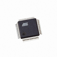
IC AVR MCU 40K 1MHZ 48LQFP
Manufacturer
Atmel
Series
AVR® ATmegar
Specifications of ATMEGA406-1AAU
Core Processor
AVR
Core Size
8-Bit
Speed
1MHz
Connectivity
I²C
Peripherals
POR, WDT
Number Of I /o
18
Program Memory Size
40KB (20K x 16)
Program Memory Type
FLASH
Eeprom Size
512 x 8
Ram Size
2K x 8
Voltage - Supply (vcc/vdd)
4 V ~ 25 V
Data Converters
A/D 10x12b
Oscillator Type
Internal
Operating Temperature
-30°C ~ 85°C
Package / Case
48-LQFP
Processor Series
ATMEGA48x
Core
AVR8
Data Bus Width
8 bit
Data Ram Size
2 KB
Interface Type
2-Wire
Maximum Clock Frequency
1 MHz
Number Of Programmable I/os
18
Number Of Timers
2
Maximum Operating Temperature
+ 85 C
Mounting Style
SMD/SMT
3rd Party Development Tools
EWAVR, EWAVR-BL
Development Tools By Supplier
ATAVRDRAGON, ATSTK500, ATSTK600, ATAVRISP2, ATAVRONEKIT
Minimum Operating Temperature
- 30 C
Cpu Family
ATmega
Device Core
AVR
Device Core Size
8b
Frequency (max)
1MHz
Total Internal Ram Size
2KB
# I/os (max)
18
Number Of Timers - General Purpose
2
Operating Supply Voltage (typ)
5/9/12/15/18/24V
Operating Supply Voltage (max)
25V
Operating Supply Voltage (min)
4V
On-chip Adc
10-chx12-bit
Instruction Set Architecture
RISC
Operating Temp Range
-30C to 85C
Operating Temperature Classification
Commercial
Mounting
Surface Mount
Pin Count
48
Package Type
LQFP
Controller Family/series
AVR MEGA
No. Of I/o's
18
Eeprom Memory Size
512Byte
Ram Memory Size
2KB
Cpu Speed
1MHz
Rohs Compliant
Yes
For Use With
770-1007 - ISP 4PORT ATMEL AVR MCU SPI/JTAG770-1005 - ISP 4PORT FOR ATMEL AVR MCU JTAG770-1004 - ISP 4PORT FOR ATMEL AVR MCU SPI
Lead Free Status / RoHS Status
Lead free / RoHS Compliant
Available stocks
Company
Part Number
Manufacturer
Quantity
Price

Part Number:
ATMEGA406-1AAU
Manufacturer:
AT
Quantity:
20 000


12.2.4
12.2.5
58
ATmega406
PCICR– Pin Change Interrupt Control Register
PCIFR – Pin Change Interrupt Flag Register
set (one), the MCU will jump to the interrupt vector. The flag is cleared when the interrupt routine
is executed. Alternatively, the flag can be cleared by writing a logical one to it. These flags are
always cleared when INT3:0 are configured as level interrupt. Note that when entering sleep
mode with the INT3:0 interrupts disabled, the input buffers on these pins will be disabled. This
may cause a logic change in internal signals which will set the INTF3:0 flags. See
Enable and Sleep Modes” on page 64
• Bit 7:2 - Res: Reserved Bits
These bits are reserved bits in the ATmega406, and will always read as zero.
• Bit 1 - PCIE1: Pin Change Interrupt Enable 1
When the PCIE1 bit is set (one) and the I-bit in the Status Register (SREG) is set (one), pin
change interrupt 1 is enabled. Any change on any enabled PCINT15:8 pin will cause an inter-
rupt. The corresponding interrupt of Pin Change Interrupt Request is executed from the PCI1
Interrupt Vector. PCINT15:8 pins are enabled individually by the PCMSK1 Register.
• Bit 0 - PCIE0: Pin Change Interrupt Enable 0
When the PCIE0 bit is set (one) and the I-bit in the Status Register (SREG) is set (one), pin
change interrupt 0 is enabled. Any change on any enabled PCINT7:0 pin will cause an interrupt.
The corresponding interrupt of Pin Change Interrupt Request is executed from the PCI0 Inter-
rupt Vector. PCINT7:0 pins are enabled individually by the PCMSK0 Register.
• Bit 7:2 - Res: Reserved Bits
These bits are reserved bits in the ATmega406, and will always read as zero.
• Bit 1 - PCIF1: Pin Change Interrupt Flag 1
When a logic change on any PCINT15:8 pin triggers an interrupt request, PCIF1 becomes set
(one). If the I-bit in SREG and the PCIE1 bit in PCICR are set (one), the MCU will jump to the
corresponding Interrupt Vector. The flag is cleared when the interrupt routine is executed. Alter-
natively, the flag can be cleared by writing a logical one to it.
• Bit 0 - PCIF0: Pin Change Interrupt Flag 0
When a logic change on any PCINT7:0 pin triggers an interrupt request, PCIF0 becomes set
(one). If the I-bit in SREG and the PCIE0 bit in PCICR are set (one), the MCU will jump to the
Bit
(0x68)
Read/Write
Initial Value
Bit
0x1B (0x3B)
Read/Write
Initial Value
R
R
7
–
0
7
–
0
R
R
6
–
0
6
–
0
R
R
5
–
0
5
–
0
for more information.
R
R
4
–
0
4
–
0
R
R
3
–
0
3
–
0
2
–
R
0
2
–
R
0
PCIE1
PCIF1
R/W
R/W
1
0
1
0
PCIE0
PCIF0
R/W
R/W
0
0
0
0
2548E–AVR–07/06
”Digital Input
PCICR
PCIFR
Related parts for ATMEGA406-1AAU
Image
Part Number
Description
Manufacturer
Datasheet
Request
R

Part Number:
Description:
Manufacturer:
Atmel Corporation
Datasheet:

Part Number:
Description:
IC AVR MCU 2.4GHZ XCEIVER 64QFN
Manufacturer:
Atmel
Datasheet:

Part Number:
Description:
Manufacturer:
Atmel
Datasheet:

Part Number:
Description:
MCU ATMEGA644/AT86RF230 40-DIP
Manufacturer:
Atmel
Datasheet:
Part Number:
Description:
BUNDLE ATMEGA644P/AT86RF230 QFN
Manufacturer:
Atmel
Datasheet:

Part Number:
Description:
BUNDLE ATMEGA644P/AT86RF230 TQFP
Manufacturer:
Atmel
Datasheet:

Part Number:
Description:
MCU ATMEGA1281/AT86RF230 64-TQFP
Manufacturer:
Atmel
Datasheet:

Part Number:
Description:
MCU ATMEGA1280/AT86RF230 100TQFP
Manufacturer:
Atmel
Datasheet:
Part Number:
Description:
BUNDLE ATMEGA1280/AT86RF100-TQFP
Manufacturer:
Atmel
Datasheet:

Part Number:
Description:
BUNDLE ATMEGA2560V/AT86RF230-ZU
Manufacturer:
Atmel
Datasheet:
Part Number:
Description:
MCU ATMEGA2561/AT86RF230 64-TQFP
Manufacturer:
Atmel
Datasheet:
Part Number:
Description:
MCU ATMEGA2560/AT86RF230 100TQFP
Manufacturer:
Atmel
Datasheet:
Part Number:
Description:
MCU ATMEGA2561/AT86RF230 64-QFN
Manufacturer:
Atmel
Datasheet:

Part Number:
Description:
MCU, 8BIT, AVR, 16K FLASH, 28PDIP
Manufacturer:
Atmel
Datasheet:

Part Number:
Description:
Microcontroller Modules MCU CARD BIGAVR6 100P W/ ATMEGA2560
Manufacturer:
mikroElektronika