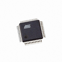
ATMEGA406-1AAU Atmel, ATMEGA406-1AAU Datasheet - Page 199

ATMEGA406-1AAU
Manufacturer Part Number
ATMEGA406-1AAU
Description
IC AVR MCU 40K 1MHZ 48LQFP
Manufacturer
Atmel
Series
AVR® ATmegar
Specifications of ATMEGA406-1AAU
Core Processor
AVR
Core Size
8-Bit
Speed
1MHz
Connectivity
I²C
Peripherals
POR, WDT
Number Of I /o
18
Program Memory Size
40KB (20K x 16)
Program Memory Type
FLASH
Eeprom Size
512 x 8
Ram Size
2K x 8
Voltage - Supply (vcc/vdd)
4 V ~ 25 V
Data Converters
A/D 10x12b
Oscillator Type
Internal
Operating Temperature
-30°C ~ 85°C
Package / Case
48-LQFP
Processor Series
ATMEGA48x
Core
AVR8
Data Bus Width
8 bit
Data Ram Size
2 KB
Interface Type
2-Wire
Maximum Clock Frequency
1 MHz
Number Of Programmable I/os
18
Number Of Timers
2
Maximum Operating Temperature
+ 85 C
Mounting Style
SMD/SMT
3rd Party Development Tools
EWAVR, EWAVR-BL
Development Tools By Supplier
ATAVRDRAGON, ATSTK500, ATSTK600, ATAVRISP2, ATAVRONEKIT
Minimum Operating Temperature
- 30 C
Cpu Family
ATmega
Device Core
AVR
Device Core Size
8b
Frequency (max)
1MHz
Total Internal Ram Size
2KB
# I/os (max)
18
Number Of Timers - General Purpose
2
Operating Supply Voltage (typ)
5/9/12/15/18/24V
Operating Supply Voltage (max)
25V
Operating Supply Voltage (min)
4V
On-chip Adc
10-chx12-bit
Instruction Set Architecture
RISC
Operating Temp Range
-30C to 85C
Operating Temperature Classification
Commercial
Mounting
Surface Mount
Pin Count
48
Package Type
LQFP
Controller Family/series
AVR MEGA
No. Of I/o's
18
Eeprom Memory Size
512Byte
Ram Memory Size
2KB
Cpu Speed
1MHz
Rohs Compliant
Yes
For Use With
770-1007 - ISP 4PORT ATMEL AVR MCU SPI/JTAG770-1005 - ISP 4PORT FOR ATMEL AVR MCU JTAG770-1004 - ISP 4PORT FOR ATMEL AVR MCU SPI
Lead Free Status / RoHS Status
Lead free / RoHS Compliant
Available stocks
Company
Part Number
Manufacturer
Quantity
Price
Part Number:
ATMEGA406-1AAU
Manufacturer:
AT
Quantity:
20 000
- Current page: 199 of 263
- Download datasheet (3Mb)
28.6
28.6.1
28.6.2
2548E–AVR–07/06
Parallel Programming
Considerations for Efficient Programming
Signal Names
This section describes parameters, pin mapping, and commands used to parallel program and
verify Flash Program memory, EEPROM Data memory, Memory Lock bits, and Fuse bits in the
ATmega406. Pulses are assumed to be at least 250 ns unless otherwise noted.
The loaded command and address are retained in the device during programming. For efficient
programming, the following should be considered.
• The command needs only be loaded once when writing or reading multiple memory locations.
• Skip writing the data value 0xFF, that is the contents of the entire EEPROM (unless the
Address high byte needs only be loaded before programming or reading a new 256 word window
in Flash or 256 byte EEPROM. This consideration also applies to Signature bytes reading.
In this section, some pins of the ATmega406 are referenced by signal names describing their
functionality during parallel programming, see
200. Pins not described in the following table are referenced by pin names.
The XA1/XA0 pins determine the action executed when the XTAL1 pin is given a positive pulse.
The bit coding is shown in
When pulsing WR or OE, the command loaded determines the action executed. The different
Commands are shown in
programming characteristics.
Figure 28-1. Parallel Programming
EESAVE Fuse is programmed) and Flash after a Chip Erase.
RDY/BSY
PAGEL
V
PP
BS2
BS1
XA0
XA1
WR
OE
Table 28-10 on page
Table 28-9 on page
RESET
XTAL1
GND
V
V
V
BATT
PVT
PV1
FET
REG
CC
Figure 28-1 on page 199
200.
201.
Table 28-11 on page 210
+4 - 25V
(3.3V)
DATA
See "Enter Programming Mode"
and
ATmega406
Table 28-7 on page
shows the Parallel
199
Related parts for ATMEGA406-1AAU
Image
Part Number
Description
Manufacturer
Datasheet
Request
R

Part Number:
Description:
Manufacturer:
Atmel Corporation
Datasheet:

Part Number:
Description:
IC AVR MCU 2.4GHZ XCEIVER 64QFN
Manufacturer:
Atmel
Datasheet:

Part Number:
Description:
Manufacturer:
Atmel
Datasheet:

Part Number:
Description:
MCU ATMEGA644/AT86RF230 40-DIP
Manufacturer:
Atmel
Datasheet:

Part Number:
Description:
BUNDLE ATMEGA644P/AT86RF230 QFN
Manufacturer:
Atmel
Datasheet:

Part Number:
Description:
BUNDLE ATMEGA644P/AT86RF230 TQFP
Manufacturer:
Atmel
Datasheet:

Part Number:
Description:
MCU ATMEGA1281/AT86RF230 64-TQFP
Manufacturer:
Atmel
Datasheet:

Part Number:
Description:
MCU ATMEGA1280/AT86RF230 100TQFP
Manufacturer:
Atmel
Datasheet:

Part Number:
Description:
BUNDLE ATMEGA1280/AT86RF100-TQFP
Manufacturer:
Atmel
Datasheet:

Part Number:
Description:
BUNDLE ATMEGA2560V/AT86RF230-ZU
Manufacturer:
Atmel
Datasheet:

Part Number:
Description:
MCU ATMEGA2561/AT86RF230 64-TQFP
Manufacturer:
Atmel
Datasheet:

Part Number:
Description:
MCU ATMEGA2560/AT86RF230 100TQFP
Manufacturer:
Atmel
Datasheet:

Part Number:
Description:
MCU ATMEGA2561/AT86RF230 64-QFN
Manufacturer:
Atmel
Datasheet:

Part Number:
Description:
MCU, 8BIT, AVR, 16K FLASH, 28PDIP
Manufacturer:
Atmel
Datasheet:

Part Number:
Description:
Microcontroller Modules MCU CARD BIGAVR6 100P W/ ATMEGA2560
Manufacturer:
mikroElektronika


