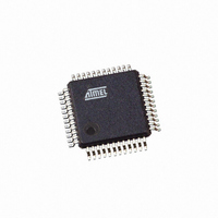
ATMEGA406-1AAU Atmel, ATMEGA406-1AAU Datasheet - Page 119

ATMEGA406-1AAU
Manufacturer Part Number
ATMEGA406-1AAU
Description
IC AVR MCU 40K 1MHZ 48LQFP
Manufacturer
Atmel
Series
AVR® ATmegar
Specifications of ATMEGA406-1AAU
Core Processor
AVR
Core Size
8-Bit
Speed
1MHz
Connectivity
I²C
Peripherals
POR, WDT
Number Of I /o
18
Program Memory Size
40KB (20K x 16)
Program Memory Type
FLASH
Eeprom Size
512 x 8
Ram Size
2K x 8
Voltage - Supply (vcc/vdd)
4 V ~ 25 V
Data Converters
A/D 10x12b
Oscillator Type
Internal
Operating Temperature
-30°C ~ 85°C
Package / Case
48-LQFP
Processor Series
ATMEGA48x
Core
AVR8
Data Bus Width
8 bit
Data Ram Size
2 KB
Interface Type
2-Wire
Maximum Clock Frequency
1 MHz
Number Of Programmable I/os
18
Number Of Timers
2
Maximum Operating Temperature
+ 85 C
Mounting Style
SMD/SMT
3rd Party Development Tools
EWAVR, EWAVR-BL
Development Tools By Supplier
ATAVRDRAGON, ATSTK500, ATSTK600, ATAVRISP2, ATAVRONEKIT
Minimum Operating Temperature
- 30 C
Cpu Family
ATmega
Device Core
AVR
Device Core Size
8b
Frequency (max)
1MHz
Total Internal Ram Size
2KB
# I/os (max)
18
Number Of Timers - General Purpose
2
Operating Supply Voltage (typ)
5/9/12/15/18/24V
Operating Supply Voltage (max)
25V
Operating Supply Voltage (min)
4V
On-chip Adc
10-chx12-bit
Instruction Set Architecture
RISC
Operating Temp Range
-30C to 85C
Operating Temperature Classification
Commercial
Mounting
Surface Mount
Pin Count
48
Package Type
LQFP
Controller Family/series
AVR MEGA
No. Of I/o's
18
Eeprom Memory Size
512Byte
Ram Memory Size
2KB
Cpu Speed
1MHz
Rohs Compliant
Yes
For Use With
770-1007 - ISP 4PORT ATMEL AVR MCU SPI/JTAG770-1005 - ISP 4PORT FOR ATMEL AVR MCU JTAG770-1004 - ISP 4PORT FOR ATMEL AVR MCU SPI
Lead Free Status / RoHS Status
Lead free / RoHS Compliant
Available stocks
Company
Part Number
Manufacturer
Quantity
Price
Part Number:
ATMEGA406-1AAU
Manufacturer:
AT
Quantity:
20 000
20.3.3
2548E–AVR–07/06
VADCL and VADCH – The V-ADC Data Register
• Bit 2 – VADSC: Voltage ADC Start Conversion
Write this bit to one to start a new conversion of the selected channel.
VADSC will read as one as long as the conversion is not finished. When the conversion is com-
plete, it returns to zero. Writing zero to this bit has no effect. VADSC will automatically be
cleared when the VADEN bit is written to zero.
• Bit 1 – VADCCIF: V-ADC Conversion Complete Interrupt Flag
This bit is set when a V-ADC conversion completes and the data registers are updated. The V-
ADC Conversion Complete Interrupt is executed if the VADCCIE bit and the I-bit in SREG are
set. VADCCIF is cleared by hardware when executing the corresponding interrupt handling vec-
tor. Alternatively, VADCCIF is cleared by writing a logical one to the flag. Beware that if doing a
Read-Modify-Write on VADCSR, a pending interrupt can be disabled.
• Bit 0 – VADCCIE: V-ADC Conversion Complete Interrupt Enable
When this bit is written to one and the I-bit in SREG is set, the V-ADC Conversion Complete
Interrupt is activated.
When a V-ADC conversion is complete, the result is found in these two registers. To ensure that
correct data is read, the data registers must be read before starting a new conversion.
• VADC11:0: V-ADC Conversion Result
These bits represent the result from the conversion.
To obtain the best absolute accuracy for the cell voltage measurements, gain and offset com-
pensation is required. Factory calibration values are stored in the device signature row, refer to
section
mV is given by:
When performing a Vtemp conversion, the result must be adjusted by the factory calibration
value stored in the signature row, refer to section
page 189
Bit
(0x79)
(0x78)
Read/Write
Initial Value
”Reading the Signature Row from Software” on page 189
Cell
for details. The absolute temperature in Kelvin is given by:
n
voltage mV
15
R
R
–
7
0
0
(
)
=
14
R
R
–
6
0
0
cell
---------------------------------------------------------------------------------------------------
T(K)
n
result cell
=
V
----------------------------------------------------------------------------------------------- -
13
R
R
–
5
0
0
temp
⋅
result VPTAT calibration word
n
TBD
gain calibration word
12
R
R
0
–
4
0
⋅
VADC[7:0]
TBD
”Reading the Signature Row from Software” on
11
R
R
3
0
0
–
10
R
R
2
0
0
cell
VADC[11:8]
n
for details. The cell voltage in
offset calibration word
R
R
9
1
0
0
ATmega406
R
R
8
0
0
0
VADCH
VADCL
119


