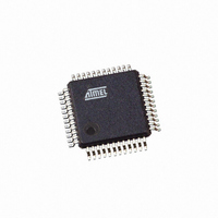
ATMEGA406-1AAU Atmel, ATMEGA406-1AAU Datasheet - Page 211

ATMEGA406-1AAU
Manufacturer Part Number
ATMEGA406-1AAU
Description
IC AVR MCU 40K 1MHZ 48LQFP
Manufacturer
Atmel
Series
AVR® ATmegar
Specifications of ATMEGA406-1AAU
Core Processor
AVR
Core Size
8-Bit
Speed
1MHz
Connectivity
I²C
Peripherals
POR, WDT
Number Of I /o
18
Program Memory Size
40KB (20K x 16)
Program Memory Type
FLASH
Eeprom Size
512 x 8
Ram Size
2K x 8
Voltage - Supply (vcc/vdd)
4 V ~ 25 V
Data Converters
A/D 10x12b
Oscillator Type
Internal
Operating Temperature
-30°C ~ 85°C
Package / Case
48-LQFP
Processor Series
ATMEGA48x
Core
AVR8
Data Bus Width
8 bit
Data Ram Size
2 KB
Interface Type
2-Wire
Maximum Clock Frequency
1 MHz
Number Of Programmable I/os
18
Number Of Timers
2
Maximum Operating Temperature
+ 85 C
Mounting Style
SMD/SMT
3rd Party Development Tools
EWAVR, EWAVR-BL
Development Tools By Supplier
ATAVRDRAGON, ATSTK500, ATSTK600, ATAVRISP2, ATAVRONEKIT
Minimum Operating Temperature
- 30 C
Cpu Family
ATmega
Device Core
AVR
Device Core Size
8b
Frequency (max)
1MHz
Total Internal Ram Size
2KB
# I/os (max)
18
Number Of Timers - General Purpose
2
Operating Supply Voltage (typ)
5/9/12/15/18/24V
Operating Supply Voltage (max)
25V
Operating Supply Voltage (min)
4V
On-chip Adc
10-chx12-bit
Instruction Set Architecture
RISC
Operating Temp Range
-30C to 85C
Operating Temperature Classification
Commercial
Mounting
Surface Mount
Pin Count
48
Package Type
LQFP
Controller Family/series
AVR MEGA
No. Of I/o's
18
Eeprom Memory Size
512Byte
Ram Memory Size
2KB
Cpu Speed
1MHz
Rohs Compliant
Yes
For Use With
770-1007 - ISP 4PORT ATMEL AVR MCU SPI/JTAG770-1005 - ISP 4PORT FOR ATMEL AVR MCU JTAG770-1004 - ISP 4PORT FOR ATMEL AVR MCU SPI
Lead Free Status / RoHS Status
Lead free / RoHS Compliant
Available stocks
Company
Part Number
Manufacturer
Quantity
Price
Part Number:
ATMEGA406-1AAU
Manufacturer:
AT
Quantity:
20 000
- Current page: 211 of 263
- Download datasheet (3Mb)
28.7
28.7.1
2548E–AVR–07/06
Programming via the JTAG Interface
Programming Specific JTAG Instructions
Programming through the JTAG interface requires control of the four JTAG specific pins: TCK,
TMS, TDI, and TDO. Control of the reset and clock pins is not required.
To be able to use the JTAG interface, the JTAGEN Fuse must be programmed. The device is
default shipped with the fuse programmed. In addition, the JTD bit in MCUCSR must be cleared.
Alternatively, if the JTD bit is set, the external reset can be forced low. Then, the JTD bit will be
cleared after two chip clocks, and the JTAG pins are available for programming. This provides a
means of using the JTAG pins as normal port pins in Running mode while still allowing In-Sys-
tem Programming via the JTAG interface. Note that this technique can not be used when using
the JTAG pins for Boundary-scan or On-chip Debug. In these cases the JTAG pins must be ded-
icated for this purpose.
As a definition in this datasheet, the LSB is shifted in and out first of all Shift Registers.
The instruction register is 4-bit wide, supporting up to 16 instructions. The JTAG instructions
useful for programming are listed below.
The OPCODE for each instruction is shown behind the instruction name in hex format. The text
describes which data register is selected as path between TDI and TDO for each instruction.
The Run-Test/Idle state of the TAP controller is used to generate internal clocks. It can also be
used as an idle state between JTAG sequences. The state machine sequence for changing the
instruction word is shown in
Figure
28-10.
ATmega406
211
Related parts for ATMEGA406-1AAU
Image
Part Number
Description
Manufacturer
Datasheet
Request
R

Part Number:
Description:
Manufacturer:
Atmel Corporation
Datasheet:

Part Number:
Description:
IC AVR MCU 2.4GHZ XCEIVER 64QFN
Manufacturer:
Atmel
Datasheet:

Part Number:
Description:
Manufacturer:
Atmel
Datasheet:

Part Number:
Description:
MCU ATMEGA644/AT86RF230 40-DIP
Manufacturer:
Atmel
Datasheet:

Part Number:
Description:
BUNDLE ATMEGA644P/AT86RF230 QFN
Manufacturer:
Atmel
Datasheet:

Part Number:
Description:
BUNDLE ATMEGA644P/AT86RF230 TQFP
Manufacturer:
Atmel
Datasheet:

Part Number:
Description:
MCU ATMEGA1281/AT86RF230 64-TQFP
Manufacturer:
Atmel
Datasheet:

Part Number:
Description:
MCU ATMEGA1280/AT86RF230 100TQFP
Manufacturer:
Atmel
Datasheet:

Part Number:
Description:
BUNDLE ATMEGA1280/AT86RF100-TQFP
Manufacturer:
Atmel
Datasheet:

Part Number:
Description:
BUNDLE ATMEGA2560V/AT86RF230-ZU
Manufacturer:
Atmel
Datasheet:

Part Number:
Description:
MCU ATMEGA2561/AT86RF230 64-TQFP
Manufacturer:
Atmel
Datasheet:

Part Number:
Description:
MCU ATMEGA2560/AT86RF230 100TQFP
Manufacturer:
Atmel
Datasheet:

Part Number:
Description:
MCU ATMEGA2561/AT86RF230 64-QFN
Manufacturer:
Atmel
Datasheet:

Part Number:
Description:
MCU, 8BIT, AVR, 16K FLASH, 28PDIP
Manufacturer:
Atmel
Datasheet:

Part Number:
Description:
Microcontroller Modules MCU CARD BIGAVR6 100P W/ ATMEGA2560
Manufacturer:
mikroElektronika


