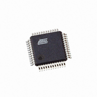
ATMEGA406-1AAU Atmel, ATMEGA406-1AAU Datasheet - Page 103

ATMEGA406-1AAU
Manufacturer Part Number
ATMEGA406-1AAU
Description
IC AVR MCU 40K 1MHZ 48LQFP
Manufacturer
Atmel
Series
AVR® ATmegar
Specifications of ATMEGA406-1AAU
Core Processor
AVR
Core Size
8-Bit
Speed
1MHz
Connectivity
I²C
Peripherals
POR, WDT
Number Of I /o
18
Program Memory Size
40KB (20K x 16)
Program Memory Type
FLASH
Eeprom Size
512 x 8
Ram Size
2K x 8
Voltage - Supply (vcc/vdd)
4 V ~ 25 V
Data Converters
A/D 10x12b
Oscillator Type
Internal
Operating Temperature
-30°C ~ 85°C
Package / Case
48-LQFP
Processor Series
ATMEGA48x
Core
AVR8
Data Bus Width
8 bit
Data Ram Size
2 KB
Interface Type
2-Wire
Maximum Clock Frequency
1 MHz
Number Of Programmable I/os
18
Number Of Timers
2
Maximum Operating Temperature
+ 85 C
Mounting Style
SMD/SMT
3rd Party Development Tools
EWAVR, EWAVR-BL
Development Tools By Supplier
ATAVRDRAGON, ATSTK500, ATSTK600, ATAVRISP2, ATAVRONEKIT
Minimum Operating Temperature
- 30 C
Cpu Family
ATmega
Device Core
AVR
Device Core Size
8b
Frequency (max)
1MHz
Total Internal Ram Size
2KB
# I/os (max)
18
Number Of Timers - General Purpose
2
Operating Supply Voltage (typ)
5/9/12/15/18/24V
Operating Supply Voltage (max)
25V
Operating Supply Voltage (min)
4V
On-chip Adc
10-chx12-bit
Instruction Set Architecture
RISC
Operating Temp Range
-30C to 85C
Operating Temperature Classification
Commercial
Mounting
Surface Mount
Pin Count
48
Package Type
LQFP
Controller Family/series
AVR MEGA
No. Of I/o's
18
Eeprom Memory Size
512Byte
Ram Memory Size
2KB
Cpu Speed
1MHz
Rohs Compliant
Yes
For Use With
770-1007 - ISP 4PORT ATMEL AVR MCU SPI/JTAG770-1005 - ISP 4PORT FOR ATMEL AVR MCU JTAG770-1004 - ISP 4PORT FOR ATMEL AVR MCU SPI
Lead Free Status / RoHS Status
Lead free / RoHS Compliant
Available stocks
Company
Part Number
Manufacturer
Quantity
Price
Part Number:
ATMEGA406-1AAU
Manufacturer:
AT
Quantity:
20 000
17. Timer/Counter0 and Timer/Counter1 Prescalers
17.1
17.2
17.3
2548E–AVR–07/06
Internal Clock Source
Prescaler Reset
External Clock Source
Timer/Counter1 and Timer/Counter0 share the same prescaler module, but the Timer/Counters
can have different prescaler settings. The description below applies to both Timer/Counter1 and
Timer/Counter0.
The Timer/Counter can be clocked directly by the system clock (by setting the CSn2:0 = 1). This
provides the fastest operation, with a maximum Timer/Counter clock frequency equal to system
clock frequency (f
clock source by setting the CSn2:0. See
Table 16-1 on page 101
either f
The prescaler is free running, i.e., operates independently of the Clock Select logic of the
Timer/Counter, and it is shared by Timer/Counter1 and Timer/Counter0. Since the prescaler is
not affected by the Timer/Counter’s clock select, the state of the prescaler will have implications
for situations where a prescaled clock is used. One example of prescaling artifacts occurs when
the timer is enabled and clocked by the prescaler (6 > CSn2:0 > 1). The number of system clock
cycles from when the timer is enabled to the first count occurs can be from 1 to N+1 system
clock cycles, where N equals the prescaler divisor.
It is possible to use the prescaler reset for synchronizing the Timer/Counter to program execu-
tion. However, care must be taken if the other Timer/Counter that shares the same prescaler
also uses prescaling. A prescaler reset will affect the prescaler period for all Timer/Counters it is
connected to.
An external clock source applied to the T0 pin can be used as Timer/Counter0 clock (clkT0). The
T0 pin is sampled once every system clock cycle by the pin synchronization logic. The synchro-
nized (sampled) signal is then passed through the edge detector.
equivalent block diagram of the T0 synchronization and edge detector logic. The registers are
clocked at the positive edge of the internal system clock (
high period of the internal system clock.
The edge detector generates one clk
= 6) edge it detects.
Figure 17-1. T1/T0 Pin Sampling
CLK_I/O
Tn
clk
I/O
/8, f
CLK_I/O
CLK_I/O
D
LE
/32, f
Q
). Alternatively, one of the taps from the prescaler can be used as a
for Timer/Counter1 settings. The prescaled clock has a frequency of
Synchronization
CLK_I/O
D
Q
/64, f
T
0
CLK_I/O
pulse for each positive (CSn2:0 = 7) or negative (CSn2:0
Table 15-9 on page 92
/128, f
CLK_I/O
/256, or f
clk
D
I/O
). The latch is transparent in the
Q
for Timer/Counter0 settings and
Figure 17-1
CLK_I/O
Edge Detector
/1024.
ATmega406
shows a functional
Tn_sync
(To Clock
Select Logic)
103


