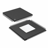
ADSP-21364BSWZ-1AA Analog Devices Inc, ADSP-21364BSWZ-1AA Datasheet - Page 33

ADSP-21364BSWZ-1AA
Manufacturer Part Number
ADSP-21364BSWZ-1AA
Description
IC DSP 32BIT 333MHZ EPAD 144LQFP
Manufacturer
Analog Devices Inc
Series
SHARC®r
Type
Fixed/Floating Pointr
Datasheet
1.ADSP-21363KSWZ-1AA.pdf
(56 pages)
Specifications of ADSP-21364BSWZ-1AA
Interface
DAI, SPI
Clock Rate
333MHz
Non-volatile Memory
ROM (512 kB)
On-chip Ram
384kB
Voltage - I/o
3.30V
Voltage - Core
1.20V
Operating Temperature
-40°C ~ 85°C
Mounting Type
Surface Mount
Package / Case
144-LQFP Exposed Pad, 144-eLQFP, 144-HLQFP
Frequency
333MHz
Supply Voltage
1.2V
Embedded Interface Type
Serial, SPI
Supply Voltage Range
1.14V To 1.26V
Operating Temperature Range
-40°C To +85°C
Digital Ic Case
RoHS Compliant
No. Of Bits
32 / 40
Rohs Compliant
Yes
Package
144LQFP EP
Numeric And Arithmetic Format
Floating-Point
Maximum Speed
333 MHz
Ram Size
384 KB
Device Million Instructions Per Second
333 MIPS
Lead Free Status / RoHS Status
Lead free / RoHS Compliant
Available stocks
Company
Part Number
Manufacturer
Quantity
Price
Company:
Part Number:
ADSP-21364BSWZ-1AA
Manufacturer:
Analog Devices Inc
Quantity:
10 000
Parallel Data Acquisition Port (PDAP)
The timing requirements for the PDAP are provided in
Table
the IDP. For details on the operation of the IDP, refer to the
ADSP-2136x SHARC Processor Hardware Reference, the chapter
“Input Data Port.”
Table 29. Parallel Data Acquisition Port (PDAP)
1
Parameter
Timing Requirements
t
t
t
t
t
t
Switching Characteristics
t
t
Data source pins are AD15–0 and DAI_P4–1, or DAI pins. Source pins for serial clock and frame sync are DAI pins.
SPCLKEN
HPCLKEN
PDSD
PDHD
PDCLKW
PDCLK
PDHLDD
PDSTRB
1
1
29. PDAP is the parallel mode operation of Channel 0 of
1
1
PDAP_CLKEN Setup Before PDAP_CLK Sample Edge
PDAP_CLKEN Hold After PDAP_CLK Sample Edge
PDAP_DAT Setup Before SCLK PDAP_CLK Sample Edge
PDAP_DAT Hold After SCLK PDAP_CLK Sample Edge
Clock Width
Clock Period
Delay of PDAP Strobe After Last PDAP_CLK Capture Edge for a Word
PDAP Strobe Pulse Width
(PDAP_STROBE)
(PDAP_CLKEN)
(PDAP_CLK)
ADSP-21362/ADSP-21363/ADSP-21364/ADSP-21365/ADSP-21366
DAI_P20–1
DAI_P20–1
DAI_P20–1
DATA
Rev. G | Page 33 of 56 | March 2011
SAMPLE EDGE
t
Figure 25. PDAP Timing
PDCLKW
t
SPCLKEN
t
PDSD
t
PDHLDD
Note that the most significant 16 bits of external 20-bit PDAP
data can be provided through either the parallel port AD15–0 or
the DAI_P20–5 pins. The remaining 4 bits can only be sourced
through DAI_P4–1. The timing below is valid at the
DAI_P20–1 pins or at the AD15–0 pins.
t
t
t
HPCLKEN
PDHD
PDCLK
t
PDSTRB
Min
2.5
2.5
3.0
2.5
(t
t
2 × t
2 × t
PCLK
PCLK
PCLK
PCLK
× 4
× 4) ÷ 2 – 3
– 1
– 1.5
Unit
ns
ns
ns
ns
ns
ns
ns
ns


