ADSP-21364BSWZ-1AA Analog Devices Inc, ADSP-21364BSWZ-1AA Datasheet - Page 18
ADSP-21364BSWZ-1AA
Manufacturer Part Number
ADSP-21364BSWZ-1AA
Description
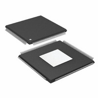
IC DSP 32BIT 333MHZ EPAD 144LQFP
Manufacturer
Analog Devices Inc
Series
SHARC®r
Type
Fixed/Floating Pointr
Datasheet
1.ADSP-21363KSWZ-1AA.pdf
(56 pages)
Specifications of ADSP-21364BSWZ-1AA
Interface
DAI, SPI
Clock Rate
333MHz
Non-volatile Memory
ROM (512 kB)
On-chip Ram
384kB
Voltage - I/o
3.30V
Voltage - Core
1.20V
Operating Temperature
-40°C ~ 85°C
Mounting Type
Surface Mount
Package / Case
144-LQFP Exposed Pad, 144-eLQFP, 144-HLQFP
Frequency
333MHz
Supply Voltage
1.2V
Embedded Interface Type
Serial, SPI
Supply Voltage Range
1.14V To 1.26V
Operating Temperature Range
-40°C To +85°C
Digital Ic Case
RoHS Compliant
No. Of Bits
32 / 40
Rohs Compliant
Yes
Package
144LQFP EP
Numeric And Arithmetic Format
Floating-Point
Maximum Speed
333 MHz
Ram Size
384 KB
Device Million Instructions Per Second
333 MIPS
Lead Free Status / RoHS Status
Lead free / RoHS Compliant
Available stocks
Company
Part Number
Manufacturer
Quantity
Price
Company:

Part Number:
ADSP-21364BSWZ-1AA
Manufacturer:
Analog Devices Inc
Quantity:
10 000


ADSP-21362/ADSP-21363/ADSP-21364/ADSP-21365/ADSP-21366
Clock Input
Table 11. Clock Input
1
2
3
4
5
6
7
Clock Signals
The processor can use an external clock or a crystal. Refer to the
CLKIN pin description in
tion program can configure the processor to use its internal
clock generator by connecting the necessary components to the
CLKIN and XTAL pins.
tions used for a fundamental frequency crystal operating in
parallel mode.
Note that the clock rate is achieved using a 16.67 MHz crystal
and a PLL multiplier ratio 16:1. (CCLK:CLKIN achieves a clock
speed of 266.72 MHz.) To achieve the full core clock rate, pro-
grams need to configure the multiplier bits in the
PMCTL register.
Parameter
Timing Requirements
t
t
t
t
t
t
t
Applies to all 200 MHz models. See
Applies to all 333 MHz models. See
Applies only for CLK_CFG1–0 = 00 and default values for PLL control bits in the PMCTL register.
Any changes to PLL control bits in the PMCTL register must meet core clock timing specification t
See
Actual input jitter should be combined with AC specifications for accurate timing analysis.
Jitter specification is maximum peak-to-peak time interval error (TIE) jitter.
CK
CKL
CKH
CKRF
CCLK
VCO
CKJ
Figure 5 on Page 16
6,7
5
4
CLKIN Period
CLKIN Width Low
CLKIN Width High
CLKIN Rise/Fall (0.4 V to 2.0 V)
CCLK Period
VCO Frequency
CLKIN Jitter Tolerance
CLKIN
for VCO diagram.
Figure 8
Table 6 on Page
Ordering Guide on Page
Ordering Guide on Page
shows the component connec-
t
CKH
11. The user applica-
54.
54.
Rev. G | Page 18 of 56 | March 2011
t
CK
t
CKL
Figure 7. Clock Input
Min
30
12.5
12.5
5.0
200
–250
3
1
1
1
200 MHz
Figure 8. Recommended Circuit for Fundamental Mode Crystal Operation
CCLK
Max
100
3
10
600
+250
.
1
C1
22pF
R2 SHOULD BE CHOSEN TO LIMIT CRYSTAL
DRIVE POWER. REFER TO CRYSTAL
MANUFACTURER’S SPECIFICATIONS.
*TYPICAL VALUES
t
CLKIN
CKJ
Min
18
7.5
7.5
3.0
200
–250
1
1
1
1
24.576MHz
R1
1M *
Y1
333 MHz
ADSP-2136x
Max
100
3
10
800
+250
XTAL
2
47
R2
C2
22pF
*
Unit
ns
ns
ns
ns
ns
MHz
ps
Related parts for ADSP-21364BSWZ-1AA
Image
Part Number
Description
Manufacturer
Datasheet
Request
R

Part Number:
Description:
±1.7g Dual-Axis IMEMS Accelerometer Evaluation Board
Manufacturer:
Analog Devices Inc
Datasheet:

Part Number:
Description:
Inertial Sensor Evaluation System
Manufacturer:
Analog Devices Inc
Datasheet:
Part Number:
Description:
Manufacturer:
Analog Devices Inc
Datasheet:
Part Number:
Description:
Manufacturer:
Analog Devices Inc
Datasheet:
Part Number:
Description:
Manufacturer:
Analog Devices Inc
Datasheet:
Part Number:
Description:
Manufacturer:
Analog Devices Inc
Datasheet:
Part Number:
Description:
Manufacturer:
Analog Devices Inc
Datasheet:
Part Number:
Description:
Manufacturer:
Analog Devices Inc
Datasheet:
Part Number:
Description:
Manufacturer:
Analog Devices Inc
Datasheet:
Part Number:
Description:
Manufacturer:
Analog Devices Inc
Datasheet:
Part Number:
Description:
Manufacturer:
Analog Devices Inc
Datasheet:
Part Number:
Description:
Manufacturer:
Analog Devices Inc
Datasheet:
Part Number:
Description:
Manufacturer:
Analog Devices Inc
Datasheet: