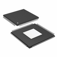
ADSP-21364BSWZ-1AA Analog Devices Inc, ADSP-21364BSWZ-1AA Datasheet - Page 25

ADSP-21364BSWZ-1AA
Manufacturer Part Number
ADSP-21364BSWZ-1AA
Description
IC DSP 32BIT 333MHZ EPAD 144LQFP
Manufacturer
Analog Devices Inc
Series
SHARC®r
Type
Fixed/Floating Pointr
Datasheet
1.ADSP-21363KSWZ-1AA.pdf
(56 pages)
Specifications of ADSP-21364BSWZ-1AA
Interface
DAI, SPI
Clock Rate
333MHz
Non-volatile Memory
ROM (512 kB)
On-chip Ram
384kB
Voltage - I/o
3.30V
Voltage - Core
1.20V
Operating Temperature
-40°C ~ 85°C
Mounting Type
Surface Mount
Package / Case
144-LQFP Exposed Pad, 144-eLQFP, 144-HLQFP
Frequency
333MHz
Supply Voltage
1.2V
Embedded Interface Type
Serial, SPI
Supply Voltage Range
1.14V To 1.26V
Operating Temperature Range
-40°C To +85°C
Digital Ic Case
RoHS Compliant
No. Of Bits
32 / 40
Rohs Compliant
Yes
Package
144LQFP EP
Numeric And Arithmetic Format
Floating-Point
Maximum Speed
333 MHz
Ram Size
384 KB
Device Million Instructions Per Second
333 MIPS
Lead Free Status / RoHS Status
Lead free / RoHS Compliant
Available stocks
Company
Part Number
Manufacturer
Quantity
Price
Company:
Part Number:
ADSP-21364BSWZ-1AA
Manufacturer:
Analog Devices Inc
Quantity:
10 000
Table 21. 16-Bit Memory Read Cycle
1
2
Parameter
Timing Requirements
t
t
Switching Characteristics
t
t
t
t
t
t
t
t
t
D = (The value set by the PPDUR Bits (5–1) in the PPCTL register) × t
H = t
F = 7 × t
On reset, ALE is an active high cycle. However, it can be configured by software to be active low.
This parameter is only available when in EMPP = 0 mode.
DRS
DRH
ALEW
ADAS
ALERW
RRH
RWALE
RDDRV
ADAH
ALEHZ1
RW
2
PCLK
1
1
PCLK
(if a hold cycle is specified, else H = 0)
(if FLASH_MODE is set, else F = 0)
AD15–0 Data Setup Before RD High
AD15–0 Data Hold After RD High
ALE Pulse Width
AD15–0 Address Setup Before ALE Deasserted
ALE Deasserted to Read Asserted
Delay Between RD Rising Edge to Next Falling
Edge
Read Deasserted to ALE Asserted
ALE Address Drive After Read High
AD15–0 Address Hold After ALE Deasserted
ALE Deasserted to Address/Data15–0 in High-Z t
RD Pulse Width
AD15–0
ALE
WR
RD
NOTE: FOR 16-BIT MEMORY READS, WHEN EMPP
ADSP-21362/ADSP-21363/ADSP-21364/ADSP-21365/ADSP-21366
WHEN EMPP = 0, MULTIPLE RD PULSES OCCUR BETWEEN ALE CYCLES. FOR COMPLETE INFORMATION,
SEE THE ADSP-2136x SHARC PROCESSOR HARDWARE REFERENCE.
t
t
ALEW
ADAS
VALID ADDRESS
t
Figure 18. Read Cycle for 16-Bit Memory Timing
ADAH
t
ALEHZ
t
ALERW
Rev. G | Page 25 of 56 | March 2011
t
t
0, ONLY ONE RD PULSE OCCURS BETWEEN ALE CYCLES.
RW
VALID DATA
Min
3.3
0
2 × t
t
2 × t
H + t
F + H + 0.5
F + H + t
t
D – 2.0
DRS
PCLK
PCLK
PCLK
PCLK
PCLK
PCLK
PCLK
– 2.5
– 2.3
t
DRH
K and B Grade
PCLK
– 2.0
– 3.8
– 1.4
t
RRH
– 2.3
VALID DATA
Max
t
PCLK
+ 3.0 t
t
RWALE
t
RDDRV
Min
4.5
0
2 × t
t
2 × t
H + t
F + H + 0.5
F + H + t
t
D – 2.0
PCLK
PCLK
PCLK
PCLK
PCLK
PCLK
– 2.5
– 2.3
PCLK
– 2.0
– 3.8
– 1.4
ADDRESS
VALID
Y Grade
– 2.3
Max
t
PCLK
+ 3.8
Unit
ns
ns
ns
ns
ns
ns
ns
ns
ns
ns
ns


