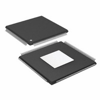
ADSP-21364BSWZ-1AA Analog Devices Inc, ADSP-21364BSWZ-1AA Datasheet - Page 16

ADSP-21364BSWZ-1AA
Manufacturer Part Number
ADSP-21364BSWZ-1AA
Description
IC DSP 32BIT 333MHZ EPAD 144LQFP
Manufacturer
Analog Devices Inc
Series
SHARC®r
Type
Fixed/Floating Pointr
Datasheet
1.ADSP-21363KSWZ-1AA.pdf
(56 pages)
Specifications of ADSP-21364BSWZ-1AA
Interface
DAI, SPI
Clock Rate
333MHz
Non-volatile Memory
ROM (512 kB)
On-chip Ram
384kB
Voltage - I/o
3.30V
Voltage - Core
1.20V
Operating Temperature
-40°C ~ 85°C
Mounting Type
Surface Mount
Package / Case
144-LQFP Exposed Pad, 144-eLQFP, 144-HLQFP
Frequency
333MHz
Supply Voltage
1.2V
Embedded Interface Type
Serial, SPI
Supply Voltage Range
1.14V To 1.26V
Operating Temperature Range
-40°C To +85°C
Digital Ic Case
RoHS Compliant
No. Of Bits
32 / 40
Rohs Compliant
Yes
Package
144LQFP EP
Numeric And Arithmetic Format
Floating-Point
Maximum Speed
333 MHz
Ram Size
384 KB
Device Million Instructions Per Second
333 MIPS
Lead Free Status / RoHS Status
Lead free / RoHS Compliant
Available stocks
Company
Part Number
Manufacturer
Quantity
Price
Company:
Part Number:
ADSP-21364BSWZ-1AA
Manufacturer:
Analog Devices Inc
Quantity:
10 000
ADSP-21362/ADSP-21363/ADSP-21364/ADSP-21365/ADSP-21366
The VCO frequency is calculated as follows:
f
f
where:
f
PLLM = Multiplier value programmed in the PMCTL register.
During reset, the PLLM value is derived from the ratio selected
using the CLK_CFG pins in hardware.
PLLN = 1, 2, 4, 8 based on the PLLD value programmed on the
PMCTL register. During reset this value is 1.
f
f
f
VCO
CCLK
VCO
INPUT
INPUT
INPUT
• The product of CLKIN and PLLM must never exceed f
(max) in
(INDIV = 1).
= 2 × PLLM × f
= VCO output
= (2 × PLLM × f
= Input frequency to the PLL.
= CLKIN when the input divider is disabled or
= CLKIN ÷ 2 when the input divider is enabled
Table 11
XTAL
INPUT
INPUT
if the input divider is enabled
BUF
CLKIN
) ÷ (2 × PLLN)
4096 CLKIN
DELAY OF
CYCLES
*CLKOUT (TEST ONLY) FREQUENCY IS THE SAME AS f
THIS SIGNAL IS NOT SPECIFIED OR SUPPORTED FOR ANY DESIGN.
DIVIDER
PMCTL
CLKIN
(INDIV)
Figure 5. Core Clock and System Clock Relationship to CLKIN
f
INPUT
Rev. G | Page 16 of 56 | March 2011
f
VCO
VCO
FILTER
LOOP
÷ (2 × PLLM)
PMCTL (2 × PLLM)
CLKOUT (TEST ONLY)*
CLK_CFGx/
PLL
VCO
Note the definitions of the clock periods that are a function of
CLKIN and the appropriate ratio control shown in
of the timing specifications for the ADSP-2136x peripherals are
defined in relation to t
tion for each peripheral’s timing information.
Table 9. Clock Periods
Figure 5
lator or crystal. The shaded divider/multiplier blocks denote
where clock ratios can be set through hardware or software
using the power management control register (PMCTL). For
more information, refer to the ADSP-2136x SHARC Processor
Hardware Reference.
Timing
Requirements
t
t
t
CK
CCLK
PCLK
INPUT.
f
VCO
shows core to CLKIN relationships with external oscil-
DIVIDER
PMCTL
(PLLD)
PLL
f
CCLK
PMCTL (CLKOUTEN)
PCLK
(PLLBP)
PMCTL
Description
CLKIN Clock Period
Processor Core Clock Period
Peripheral Clock Period = 2 × t
. Refer to the peripheral specific sec-
DIVIDE
BY 2
BUF
CCLK
PCLK
Table
CCLK
9. All


