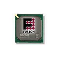
AFS600-FGG484 Actel, AFS600-FGG484 Datasheet - Page 80

AFS600-FGG484
Manufacturer Part Number
AFS600-FGG484
Description
FPGA - Field Programmable Gate Array 600K System Gates
Manufacturer
Actel
Datasheet
1.AFS600-PQG208.pdf
(330 pages)
Specifications of AFS600-FGG484
Processor Series
AFS600
Core
IP Core
Maximum Operating Frequency
1098.9 MHz
Number Of Programmable I/os
172
Data Ram Size
110592
Supply Voltage (max)
1.575 V
Maximum Operating Temperature
+ 70 C
Minimum Operating Temperature
0 C
Development Tools By Supplier
AFS-Eval-Kit, AFS-BRD600, FlashPro 3, FlashPro Lite, Silicon-Explorer II, Silicon-Sculptor 3, SI-EX-TCA
Mounting Style
SMD/SMT
Supply Voltage (min)
1.425 V
Number Of Gates
600 K
Package / Case
FPBGA-484
Lead Free Status / RoHS Status
Lead free / RoHS Compliant
Available stocks
Company
Part Number
Manufacturer
Quantity
Price
Company:
Part Number:
AFS600-FGG484
Manufacturer:
Actel
Quantity:
135
Company:
Part Number:
AFS600-FGG484I
Manufacturer:
Microsemi SoC
Quantity:
10 000
Part Number:
AFS600-FGG484I
Manufacturer:
MICROSEMI/美高森美
Quantity:
20 000
Company:
Part Number:
AFS600-FGG484K
Manufacturer:
Microsemi SoC
Quantity:
10 000
- Current page: 80 of 330
- Download datasheet (13Mb)
Device Architecture
2- 64
RAM512X18 exhibits slightly different behavior from RAM4K9, as it has dedicated read and write ports.
WW and RW
These signals enable the RAM to be configured in one of the two allowable aspect ratios
Table 2-30 • Aspect Ratio Settings for WW[1:0]
WD and RD
These are the input and output data signals, and they are 18 bits wide. When a 512×9 aspect ratio is
used for write, WD[17:9] are unused and must be grounded. If this aspect ratio is used for read, then
RD[17:9] are undefined.
WADDR and RADDR
These are read and write addresses, and they are nine bits wide. When the 256×18 aspect ratio is used
for write or read, WADDR[8] or RADDR[8] are unused and must be grounded.
WCLK and RCLK
These signals are the write and read clocks, respectively. They are both active high.
WEN and REN
These signals are the write and read enables, respectively. They are both active low by default. These
signals can be configured as active high.
RESET
This active low signal resets the output to zero, disables reads and/or writes from the SRAM block, and
clears the data hold registers when asserted. It does not reset the contents of the memory.
PIPE
This signal is used to specify pipelined read on the output. A Low on PIPE indicates a nonpipelined read,
and the data appears on the output in the same clock cycle. A High indicates a pipelined read, and data
appears on the output in the next clock cycle.
Clocking
The dual-port SRAM blocks are only clocked on the rising edge. SmartGen allows falling-edge-triggered
clocks by adding inverters to the netlist, hence achieving dual-port SRAM blocks that are clocked on
either edge (rising or falling). For dual-port SRAM, each port can be clocked on either edge or by
separate clocks, by port.
Fusion devices support inversion (bubble pushing) throughout the FPGA architecture, including the clock
input to the SRAM modules. Inversions added to the SRAM clock pin on the design schematic or in the
HDL code will be automatically accounted for during design compile without incurring additional delay in
the clock path.
The two-port SRAM can be clocked on the rising edge or falling edge of WCLK and RCLK.
If negative-edge RAM and FIFO clocking is selected for memory macros, clock edge inversion
management (bubble pushing) is automatically used within the Fusion development tools, without
performance penalty.
WW[1:0]
01
10
00, 11
R e visio n 1
RW[1:0]
00, 11
01
10
Reserved
256×18
512×9
D×W
(Table
2-30).
Related parts for AFS600-FGG484
Image
Part Number
Description
Manufacturer
Datasheet
Request
R

Part Number:
Description:
AFS600-1FGG256I
Manufacturer:
Actel
Datasheet:

Part Number:
Description:
AFS600-2FGG256I
Manufacturer:
Actel
Datasheet:


