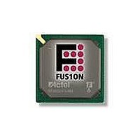
AFS600-FGG484 Actel, AFS600-FGG484 Datasheet - Page 120

AFS600-FGG484
Manufacturer Part Number
AFS600-FGG484
Description
FPGA - Field Programmable Gate Array 600K System Gates
Manufacturer
Actel
Datasheet
1.AFS600-PQG208.pdf
(330 pages)
Specifications of AFS600-FGG484
Processor Series
AFS600
Core
IP Core
Maximum Operating Frequency
1098.9 MHz
Number Of Programmable I/os
172
Data Ram Size
110592
Supply Voltage (max)
1.575 V
Maximum Operating Temperature
+ 70 C
Minimum Operating Temperature
0 C
Development Tools By Supplier
AFS-Eval-Kit, AFS-BRD600, FlashPro 3, FlashPro Lite, Silicon-Explorer II, Silicon-Sculptor 3, SI-EX-TCA
Mounting Style
SMD/SMT
Supply Voltage (min)
1.425 V
Number Of Gates
600 K
Package / Case
FPBGA-484
Lead Free Status / RoHS Status
Lead free / RoHS Compliant
Available stocks
Company
Part Number
Manufacturer
Quantity
Price
Company:
Part Number:
AFS600-FGG484
Manufacturer:
Actel
Quantity:
135
Company:
Part Number:
AFS600-FGG484I
Manufacturer:
Microsemi SoC
Quantity:
10 000
Part Number:
AFS600-FGG484I
Manufacturer:
MICROSEMI/美高森美
Quantity:
20 000
Company:
Part Number:
AFS600-FGG484K
Manufacturer:
Microsemi SoC
Quantity:
10 000
- Current page: 120 of 330
- Download datasheet (13Mb)
Device Architecture
2- 10 4
ADC Configuration Description
The Fusion ADC can be configured to operate in 8-, 10-, or 12-bit modes, power-down after conversion,
and dynamic calibration. This is controlled by MODE[3:0], as defined in
The output of the ADC is the RESULT[11:0] signal. In 8-bit mode, the Most Significant 8 Bits
RESULT[11:4] are used as the ADC value and the Least Significant 4 Bits RESULT[3:0] are logical '0's.
In 10-bit mode, RESULT[11:2] are used the ADC value and RESULT[1:0] are logical '0's.
Table 2-41 • Mode Bits Function
The speed of the ADC depends on its internal clock, ADCCLK, which is not accessible to users. The
ADCCLK is derived from SYSCLK. Input signal TVC[7:0], Time Divider Control, determines the speed of
the ADCCLK in relationship to SYSCLK, based on
Table 2-42 • TVC Bits Function
The frequency of ADCCLK, f
The inputs to the ADC are synchronized to SYSCLK. A conversion is initiated by asserting the
ADCSTART signal on a rising edge of SYSCLK.
page 2-109
A conversion is performed in three phases. In the first phase, the analog input voltage is sampled on the
input capacitor. This phase is called sample phase. During the sample phase, the output signals BUSY
and SAMPLE change from '0' to '1', indicating the ADC is busy and sampling the analog signal. The
sample time can be controlled by input signals STC[7:0]. The sample time can be calculated by
When controlling the sample time for the ADC along with the use of Prescaler or Current Monitor or
Temperature Monitor, the minimum sample time for each must be obeyed. Refer to the corresponding
section and
Name
MODE
MODE
MODE
Name
TVC
TVC: Time Divider Control (0–255)
t
t
STC: Sample Time Control value (0–255)
ADCCLK
SYSCLK
is the period of SYSCLK
show the timing diagram for the ADC.
is the period of ADCCLK, and must be between 0.5 MHz and 10 MHz
Table 2-43
Bits
1:0
3
2
for further information.
0 – Internal calibration after every conversion; two ADCCLK cycles are used
after the conversion.
1 – No calibration after every conversion
0 – Power-down after conversion
1 – No Power-down after conversion
00 – 10-bit
01 – 12-bit
10 – 8-bit
11 – Unused
ADCCLK
t
ADCCLK
, must be within 0.5 Hz to 10 MHz.
t
sample
=
=
R e visio n 1
4
(
Bits
[7:0]
×
2
(
+
1
EQ
STC
+
TVC
Figure 2-83 on page 2-108
11.
)
×
)
Function
t
ADCCLK
×
t
SYSCLK
SYSCLK divider control
Table 2-41 on page
Function
and
Figure 2-84 on
2-104.
EQ
EQ 12
EQ 11
12.
Related parts for AFS600-FGG484
Image
Part Number
Description
Manufacturer
Datasheet
Request
R

Part Number:
Description:
AFS600-1FGG256I
Manufacturer:
Actel
Datasheet:

Part Number:
Description:
AFS600-2FGG256I
Manufacturer:
Actel
Datasheet:


