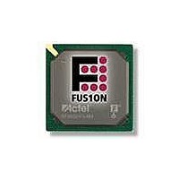
AFS600-FGG484 Actel, AFS600-FGG484 Datasheet - Page 46

AFS600-FGG484
Manufacturer Part Number
AFS600-FGG484
Description
FPGA - Field Programmable Gate Array 600K System Gates
Manufacturer
Actel
Datasheet
1.AFS600-PQG208.pdf
(330 pages)
Specifications of AFS600-FGG484
Processor Series
AFS600
Core
IP Core
Maximum Operating Frequency
1098.9 MHz
Number Of Programmable I/os
172
Data Ram Size
110592
Supply Voltage (max)
1.575 V
Maximum Operating Temperature
+ 70 C
Minimum Operating Temperature
0 C
Development Tools By Supplier
AFS-Eval-Kit, AFS-BRD600, FlashPro 3, FlashPro Lite, Silicon-Explorer II, Silicon-Sculptor 3, SI-EX-TCA
Mounting Style
SMD/SMT
Supply Voltage (min)
1.425 V
Number Of Gates
600 K
Package / Case
FPBGA-484
Lead Free Status / RoHS Status
Lead free / RoHS Compliant
Available stocks
Company
Part Number
Manufacturer
Quantity
Price
Company:
Part Number:
AFS600-FGG484
Manufacturer:
Actel
Quantity:
135
Company:
Part Number:
AFS600-FGG484I
Manufacturer:
Microsemi SoC
Quantity:
10 000
Part Number:
AFS600-FGG484I
Manufacturer:
MICROSEMI/美高森美
Quantity:
20 000
Company:
Part Number:
AFS600-FGG484K
Manufacturer:
Microsemi SoC
Quantity:
10 000
- Current page: 46 of 330
- Download datasheet (13Mb)
Device Architecture
Table 2-12 • Fusion CCC/PLL Specification
2- 30
Parameter
Clock Conditioning Circuitry Input Frequency f
Clock Conditioning Circuitry Output Frequency f
Delay Increments in Programmable Delay Blocks
Number of Programmable Values in Each Programmable
Delay Block
Input Period Jitter
CCC Output Peak-to-Peak Period Jitter F
Acquisition Time
Tracking Jitter
Output Duty Cycle
Delay Range in Block: Programmable Delay 1
Delay Range in Block: Programmable Delay 2
Delay Range in Block: Fixed Delay
Notes:
1. This delay is a function of voltage and temperature. See
2. T
3. Tracking jitter is defined as the variation in clock edge position of PLL outputs with reference to PLL input clock edge.
0.75 MHz to 24 MHz
24 MHz to 100 MHz
100 MHz to 250 MHz
250 MHz to 350 MHz
Tracking jitter does not measure the variation in PLL output period, which is covered by period jitter parameter.
J
= 25°C, VCC = 1.5 V
CCC and PLL Characteristics
Timing Characteristics
3
1, 2
CCC_OUT
LockControl = 0
LockControl = 1
LockControl = 0
LockControl = 1
IN_CCC
1, 2
1, 2
OUT_CCC
1, 2
Table 3-7 on page 3-9
R e visio n 1
1 Global
Network
1.00%
1.50%
2.25%
3.50%
0.025
Used
Min.
0.75
48.5
Max Peak-to-Peak Period Jitter
1.5
0.6
for deratings.
Typ.
160
2.2
Networks
3 Global
1.00%
1.50%
2.25%
3.50%
Max.
Used
51.5
5.56
5.56
350
350
300
1.5
6.0
1.6
0.8
32
MHz
MHz
Unit
ms
ps
ns
µs
ns
ns
ns
ns
ns
%
Related parts for AFS600-FGG484
Image
Part Number
Description
Manufacturer
Datasheet
Request
R

Part Number:
Description:
AFS600-1FGG256I
Manufacturer:
Actel
Datasheet:

Part Number:
Description:
AFS600-2FGG256I
Manufacturer:
Actel
Datasheet:


