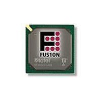
AFS600-FGG484 Actel, AFS600-FGG484 Datasheet - Page 227

AFS600-FGG484
Manufacturer Part Number
AFS600-FGG484
Description
FPGA - Field Programmable Gate Array 600K System Gates
Manufacturer
Actel
Datasheet
1.AFS600-PQG208.pdf
(330 pages)
Specifications of AFS600-FGG484
Processor Series
AFS600
Core
IP Core
Maximum Operating Frequency
1098.9 MHz
Number Of Programmable I/os
172
Data Ram Size
110592
Supply Voltage (max)
1.575 V
Maximum Operating Temperature
+ 70 C
Minimum Operating Temperature
0 C
Development Tools By Supplier
AFS-Eval-Kit, AFS-BRD600, FlashPro 3, FlashPro Lite, Silicon-Explorer II, Silicon-Sculptor 3, SI-EX-TCA
Mounting Style
SMD/SMT
Supply Voltage (min)
1.425 V
Number Of Gates
600 K
Package / Case
FPBGA-484
Lead Free Status / RoHS Status
Lead free / RoHS Compliant
Available stocks
Company
Part Number
Manufacturer
Quantity
Price
Company:
Part Number:
AFS600-FGG484
Manufacturer:
Actel
Quantity:
135
Company:
Part Number:
AFS600-FGG484I
Manufacturer:
Microsemi SoC
Quantity:
10 000
Part Number:
AFS600-FGG484I
Manufacturer:
MICROSEMI/美高森美
Quantity:
20 000
Company:
Part Number:
AFS600-FGG484K
Manufacturer:
Microsemi SoC
Quantity:
10 000
- Current page: 227 of 330
- Download datasheet (13Mb)
Figure 2-132 • LVDS Circuit Diagram and Board-Level Implementation
Table 2-165 • Minimum and Maximum DC Input and Output Levels
DC Parameter
VCCI
VOL
VOH
I
I
V
I
I
V
V
V
V
Notes:
1. ±5%
2. Differential input voltage = ±350 mV
3. I
4. Currents are measured at 85°C junction temperature.
5. I
6. I
OL
OH
IL
IH
I
ODIFF
OCM
ICM
IDIFF
OUTBUF_LVDS
4,5
4,6
3
larger when operating outside recommended ranges.
3
OL
IL
IH
is the input leakage current per I/O pin over recommended operation conditions where –0.3 V < VIN < VIL.
/I
is the input leakage current per I/O pin over recommended operating conditions VIH < VIN < VCCI. Input current is
OH
defined by V
Differential I/O Characteristics
Configuration of the I/O modules as a differential pair is handled by the Actel Designer software
when the user instantiates a differential I/O macro in the design.
Differential I/Os can also be used in conjunction with the embedded Input Register (InReg), Output
Register (OutReg), Enable Register (EnReg), and Double Data Rate (DDR). However, there is no
support for bidirectional I/Os or tristates with these standards.
LVDS
Low-Voltage Differential Signal (ANSI/TIA/EIA-644) is a high-speed differential I/O standard. It requires
that one data bit be carried through two signal lines, so two pins are needed. It also requires external
resistor termination.
The full implementation of the LVDS transmitter and receiver is shown in an example in
The building blocks of the LVDS transmitter–receiver are one transmitter macro, one receiver macro,
three board resistors at the transmitter end, and one resistor at the receiver end. The values for the three
driver resistors are different from those used in the LVPECL implementation because the output
standard specifications are different.
Supply Voltage
Output Low Voltage
Input High Voltage
Output Low Voltage
Output High Voltage
Input Voltage
Input Low Voltage
Input High Voltage
Differential Output Voltage
Output Common Mode Voltage
Input Common Mode Voltage
Input Differential Voltage
FPGA
ODIFF
/(Resistor Network)
Description
P
N
Bourns Part Number: CAT16-LV4F12
165 Ω
165 Ω
140 Ω
R e v i s i o n 1
2.375
1.125
Min.
0.65
0.65
ZO = 50 Ω
ZO = 50 Ω
1.25
0.05
250
100
0.9
0
100 Ω
1.075
1.425
Typ.
0.91
0.91
1.25
1.25
350
350
2.5
Actel Fusion Family of Mixed Signal FPGAs
N
P
FPGA
Max.
2.625
2.925
1.375
+
1.16
1.16
–
1.25
2.35
450
1.6
10
10
INBUF_LVDS
Figure
Units
mV
mV
mA
mA
μA
μA
V
V
V
V
V
V
2-132.
2- 211
Related parts for AFS600-FGG484
Image
Part Number
Description
Manufacturer
Datasheet
Request
R

Part Number:
Description:
AFS600-1FGG256I
Manufacturer:
Actel
Datasheet:

Part Number:
Description:
AFS600-2FGG256I
Manufacturer:
Actel
Datasheet:


