MFRC50001T/0FE,112 NXP Semiconductors, MFRC50001T/0FE,112 Datasheet - Page 87
MFRC50001T/0FE,112
Manufacturer Part Number
MFRC50001T/0FE,112
Description
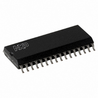
IC MIFARE READER 32-SOIC
Manufacturer
NXP Semiconductors
Series
MIFARE®r
Specifications of MFRC50001T/0FE,112
Rf Type
Read Only
Frequency
13.56MHz
Features
ISO14443-A, ISO14443-B, ISO15693
Package / Case
32-SOIC (0.300", 7.50mm Width)
Product
RFID Readers
Operating Temperature Range
- 25 C to + 85 C
Lead Free Status / RoHS Status
Lead free / RoHS Compliant
Lead Free Status / RoHS Status
Lead free / RoHS Compliant, Lead free / RoHS Compliant
Other names
568-2222-5
935268039112
MFRC500
MFRC51T0FED
935268039112
MFRC500
MFRC51T0FED
Available stocks
Company
Part Number
Manufacturer
Quantity
Price

Part Number:
MFRC50001T/0FE,112
Manufacturer:
NXP/恩智浦
Quantity:
20 000


NXP Semiconductors
MFRC500_33
Product data sheet
PUBLIC
13.4.2 Common read/write strobe bus timing
Remark: The signal ALE is not relevant for separate address/data bus and the
multiplexed addresses on the data bus do not care. The multiplexed address and data bus
address lines (A0 to A2) must be connected as described in
Table 156. Common read/write strobe timing specification
Symbol
t
t
t
t
t
t
t
t
t
t
t
t
LHLL
AVLL
LLAX
LLDSL
SLDSL
DSHSH
DSLDV
DSHDZ
DSLQV
DSHQX
DSHRWX
DSLDSH
Fig 19. Separate read/write strobe timing diagram
D0 to D7
A0 to A2
NWR
NCS
NRD
ALE
Parameter
ALE HIGH time
address valid to ALE LOW time
address hold after ALE LOW time
ALE LOW to data strobe LOW time
chip select LOW to data strobe
LOW time
data strobe HIGH to chip select
HIGH time
data strobe LOW to data input valid
time
data strobe HIGH to data input high
impedance time
data strobe LOW to data output
valid time
data output hold after data strobe
HIGH time
RW hold after data strobe HIGH
time
data strobe LOW time
All information provided in this document is subject to legal disclaimers.
Rev. 3.3 — 15 March 2010
Multiplexed address bus
t
RWHRWL
t
LHLL
t
AVLL
A0 to A2
048033
t
LLAX
Highly Integrated ISO/IEC 14443 A Reader IC
t
LLRWL
t
AVRWL
t
SLRWL
Conditions
NWR or NRD
LOW
NCS LOW to
NDS LOW
NDS/NCS LOW
NDS HIGH (write
cycle hold time)
after NDS HIGH
NDS/NCS
Separated address bus
A0 to A2
t
t
WLQV
RLDV
Section 9.1.3 on page
t
RWLRWH
D0 to D7
Min
20
15
8
15
0
0
-
-
-
8
8
65
MFRC500
© NXP B.V. 2010. All rights reserved.
-
Typ Max Unit
-
-
-
-
-
-
-
-
-
-
-
t
RWHRWL
t
t
t
WHDX
t
RHDZ
RWHSH
WHAX
-
-
-
-
-
-
65
20
35
-
-
-
001aaj638
87 of 110
8.
ns
ns
ns
ns
ns
ns
ns
ns
ns
ns
ns
ns
Related parts for MFRC50001T/0FE,112
Image
Part Number
Description
Manufacturer
Datasheet
Request
R

Part Number:
Description:
NXP Semiconductors designed the LPC2420/2460 microcontroller around a 16-bit/32-bitARM7TDMI-S CPU core with real-time debug interfaces that include both JTAG andembedded trace
Manufacturer:
NXP Semiconductors
Datasheet:

Part Number:
Description:
NXP Semiconductors designed the LPC2458 microcontroller around a 16-bit/32-bitARM7TDMI-S CPU core with real-time debug interfaces that include both JTAG andembedded trace
Manufacturer:
NXP Semiconductors
Datasheet:
Part Number:
Description:
NXP Semiconductors designed the LPC2468 microcontroller around a 16-bit/32-bitARM7TDMI-S CPU core with real-time debug interfaces that include both JTAG andembedded trace
Manufacturer:
NXP Semiconductors
Datasheet:
Part Number:
Description:
NXP Semiconductors designed the LPC2470 microcontroller, powered by theARM7TDMI-S core, to be a highly integrated microcontroller for a wide range ofapplications that require advanced communications and high quality graphic displays
Manufacturer:
NXP Semiconductors
Datasheet:
Part Number:
Description:
NXP Semiconductors designed the LPC2478 microcontroller, powered by theARM7TDMI-S core, to be a highly integrated microcontroller for a wide range ofapplications that require advanced communications and high quality graphic displays
Manufacturer:
NXP Semiconductors
Datasheet:
Part Number:
Description:
The Philips Semiconductors XA (eXtended Architecture) family of 16-bit single-chip microcontrollers is powerful enough to easily handle the requirements of high performance embedded applications, yet inexpensive enough to compete in the market for hi
Manufacturer:
NXP Semiconductors
Datasheet:
Part Number:
Description:
The XA-S3 device is a member of Philips Semiconductors? XA(eXtended Architecture) family of high performance 16-bitsingle-chip microcontrollers
Manufacturer:
NXP Semiconductors
Datasheet:

Part Number:
Description:
The NXP BlueStreak LH75401/LH75411 family consists of two low-cost 16/32-bit System-on-Chip (SoC) devices
Manufacturer:
NXP Semiconductors
Datasheet:
Part Number:
Description:
The NXP LPC3130/3131 combine an 180 MHz ARM926EJ-S CPU core, high-speed USB2
Manufacturer:
NXP Semiconductors
Datasheet:
Part Number:
Description:
The NXP LPC3141 combine a 270 MHz ARM926EJ-S CPU core, High-speed USB 2
Manufacturer:
NXP Semiconductors
Part Number:
Description:
The NXP LPC3143 combine a 270 MHz ARM926EJ-S CPU core, High-speed USB 2
Manufacturer:
NXP Semiconductors

Part Number:
Description:
The NXP LPC3152 combines an 180 MHz ARM926EJ-S CPU core, High-speed USB 2
Manufacturer:
NXP Semiconductors
Part Number:
Description:
The NXP LPC3154 combines an 180 MHz ARM926EJ-S CPU core, High-speed USB 2
Manufacturer:
NXP Semiconductors

Part Number:
Description:
Standard level N-channel enhancement mode Field-Effect Transistor (FET) in a plastic package using NXP High-Performance Automotive (HPA) TrenchMOS technology
Manufacturer:
NXP Semiconductors
Datasheet: