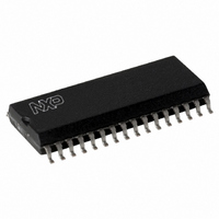
MFRC50001T/0FE,112 NXP Semiconductors, MFRC50001T/0FE,112 Datasheet - Page 5

MFRC50001T/0FE,112
Manufacturer Part Number
MFRC50001T/0FE,112
Description
IC MIFARE READER 32-SOIC
Manufacturer
NXP Semiconductors
Series
MIFARE®r
Specifications of MFRC50001T/0FE,112
Rf Type
Read Only
Frequency
13.56MHz
Features
ISO14443-A, ISO14443-B, ISO15693
Package / Case
32-SOIC (0.300", 7.50mm Width)
Product
RFID Readers
Operating Temperature Range
- 25 C to + 85 C
Lead Free Status / RoHS Status
Lead free / RoHS Compliant
Lead Free Status / RoHS Status
Lead free / RoHS Compliant, Lead free / RoHS Compliant
Other names
568-2222-5
935268039112
MFRC500
MFRC51T0FED
935268039112
MFRC500
MFRC51T0FED
Available stocks
Company
Part Number
Manufacturer
Quantity
Price
Part Number:
MFRC50001T/0FE,112
Manufacturer:
NXP/恩智浦
Quantity:
20 000
NXP Semiconductors
8. Pinning information
Table 3.
MFRC500_33
Product data sheet
PUBLIC
Pin
1
2
3
4
5
6
7
8
9
10
11
[2]
[3]
[3]
Pin description
Symbol
OSCIN
IRQ
MFIN
MFOUT
TX1
TVDD
TX2
TVSS
NCS
NWR
R/NW
nWrite
NRD
NDS
nDStrb
8.1 Pin description
Fig 2.
Type
I
O
I
O
O
P
O
G
I
I
I
I
I
I
I
[1]
MFRC500 pin configuration
Description
oscillator/clock inputs:
interrupt request: generates an output signaling an interrupt event
ISO/IEC 14443 A MIFARE serial data interface input
serial data ISO/IEC 14443 A output
transmitter 1 modulated carrier output; 13.56 MHz
transmitter power supply for the TX1 and TX2 output stages
transmitter 2 modulated carrier output; 13.56 MHz
transmitter ground for the TX1 and TX2 output stages
not chip select input is used to select and activate the MFRC500’s microprocessor
interface
registers when applied to pins D0 to D7
read not write input is used to switch between read or write cycles
not write input selects the read or write cycle to be performed
not read input generates the strobe signal for reading data from the MFRC500
registers when applied to pins D0 to D7
not data strobe input generates the strobe signal for the read and write cycles
not data strobe input generates the strobe signal for the read and write cycles
not write input generates the strobe signal for writing data to the MFRC500
All information provided in this document is subject to legal disclaimers.
crystal oscillator input to the oscillator’s inverting amplifier
externally generated clock input; f
NWR/R/NW/nWrite
NRD/NDS/nDStrb
Rev. 3.3 — 15 March 2010
MFOUT
AD0/D0
AD1/D1
AD2/D2
AD3/D3
OSCIN
TVDD
DVSS
TVSS
MFIN
048033
NCS
TX1
TX2
IRQ
10
11
12
13
14
15
16
1
2
3
4
5
6
7
8
9
Highly Integrated ISO/IEC 14443 A Reader IC
MFRC500
clk(ext)
001aal483
= 13.56 MHz
32
31
30
29
28
27
26
25
24
23
22
21
20
19
18
17
OSCOUT
RSTPD
VMID
RX
AVSS
AUX
AVDD
DVDD
A2
A1
A0/nWait
ALE/AS/nAStrb
D7/AD7
D6/AD6
D5/AD5
D4/AD4
MFRC500
© NXP B.V. 2010. All rights reserved.
5 of 110


