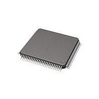
71M6534-IGT/F Maxim Integrated Products, 71M6534-IGT/F Datasheet - Page 58

71M6534-IGT/F
Manufacturer Part Number
71M6534-IGT/F
Description
IC ENERY METER 3PH 128K 120-LQFP
Manufacturer
Maxim Integrated Products
Datasheet
1.71M6533H-IGTF.pdf
(132 pages)
Specifications of 71M6534-IGT/F
Mounting Style
SMD/SMT
Package / Case
LQFP-120
Lead Free Status / RoHS Status
Lead free / RoHS Compliant
Available stocks
Company
Part Number
Manufacturer
Quantity
Price
Company:
Part Number:
71M6534-IGT/F
Manufacturer:
HONEYWELL
Quantity:
10
Company:
Part Number:
71M6534-IGT/F
Manufacturer:
Maxim Integrated
Quantity:
10 000
Part Number:
71M6534-IGT/F
Manufacturer:
MAXIM/美信
Quantity:
20 000
To facilitate transition to SLEEP mode, which is useful when an unprogrammed IC is mounted on a PCB
with a battery installed, the Teridian production test programs the following six-byte sequence into the
flash location starting at address 0x00000: 0x74 - 0x40 - 0x90 - 0x20 - 0xA9 - 0xF0. This sequence
decodes to the following assembler code:
0000: 7440
0002: 9020A9
0005: F0
Transitions from both LCD and SLEEP mode are initiated by wake-up timer timeout conditions or
pushbutton events. When the PB pin is pulled high (pushbutton is pressed), the IE_PB interrupt flag (SFR
0xE8[4]) is set, and when the wake-up timer times out, the IE_WAKE interrupt flag (SFR 0xE8[5]) is set.
In the absence of system power, if the voltage margin for the LDO regulator providing 2.5 V to the internal
circuitry becomes too low to be safe, the part automatically enters SLEEP mode (BAT_OK false). The
battery voltage must stay above 3 V to ensure that BAT_OK remains true. Under this condition, the
71M6533 and 71M6534 stays in SLEEP mode, even if the voltage margin for the LDO improves (BAT_OK
true).
58
Circuit Function
CE
CE/MPU Data RAM
FIR
Analog circuits:
MPU clock rate
MPU_DIV
ICE
DIO Pins
Watchdog Timer
LCD
EEPROM Interface (2-wire)
EEPROM Interface (3-wire)
UART
Optical TX modulation
Flash Read
Flash Page Erase
Flash Write
XRAM Read and Write
Wakeup Timer
Oscillator and RTC
XRAM data preservation
V3P3D voltage output pin
GPO – GP7 registers
– indicates not active
Table 50
shows the circuit functions available in each operating mode.
MOV A,#40
MOV DPTR,#20A9
MOVX @DPTR,A
Table 50: Available Circuit Functions
System Power
MPU_DIV[2:0]
From PLL, as
defined by
MISSION
; set bit 6 in accumulator
; point to I/O RAM address 0x20A9
; set bit 6 (sleep) in 0x20A9
Yes
Yes
Yes
Yes
Yes
Yes
Yes
Yes
Yes
Yes
Yes
Yes
Yes
Yes
Yes
Yes
Yes
Yes
Yes
Yes
Yes
Yes
(7/8 of 32768 Hz)
Yes (16 kb/s)
BROWNOUT
Yes (8 kb/s)
28.672 kHz
Battery Power (Nonvolatile Supply)
300 bd
Yes
Yes
Yes
Yes
Yes
Yes
Yes
Yes
Yes
Yes
Yes
Yes
Yes
–
–
–
–
–
–
LCD
Yes
Yes
Yes
Yes
–
–
–
–
–
–
–
–
–
–
–
–
–
–
–
–
–
–
–
SLEEP
Yes
Yes
Yes
–
–
–
–
–
–
–
–
–
–
–
–
–
–
–
–
–
–
–
–
Rev 2


