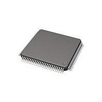
71M6534-IGT/F Maxim Integrated Products, 71M6534-IGT/F Datasheet - Page 10

71M6534-IGT/F
Manufacturer Part Number
71M6534-IGT/F
Description
IC ENERY METER 3PH 128K 120-LQFP
Manufacturer
Maxim Integrated Products
Datasheet
1.71M6533H-IGTF.pdf
(132 pages)
Specifications of 71M6534-IGT/F
Mounting Style
SMD/SMT
Package / Case
LQFP-120
Lead Free Status / RoHS Status
Lead free / RoHS Compliant
Available stocks
Company
Part Number
Manufacturer
Quantity
Price
Company:
Part Number:
71M6534-IGT/F
Manufacturer:
HONEYWELL
Quantity:
10
Company:
Part Number:
71M6534-IGT/F
Manufacturer:
Maxim Integrated
Quantity:
10 000
Part Number:
71M6534-IGT/F
Manufacturer:
MAXIM/美信
Quantity:
20 000
1.2.2 Input Multiplexer
The input multiplexer applies the input signals from the pins IAP/IAN, VA, IBP/IBN, VB, ICP/ICN, VC, and
IDP/IDN to the input of the ADC. Additionally, using the alternate multiplexer selection, it has the ability to
select temperature and the battery voltage. One input is applied per time slot.
The multiplexer can implement from one to 10 time slots (states) per frame as controlled by the I/O RAM
field MUX_DIV[3:0]. The multiplexer always starts at state 1 and proceeds until as many states as defined
by MUX_DIV[3:0] have been converted.
The multiplexer can be operated in two modes:
•
•
The alternate multiplexer cycles are usually performed infrequently (every second or so) by the MPU. In
order to prevent disruption of the voltage tracking mechanism and voltage allpass networks of the CE,
VA, VB, and VC are not replaced in the alternate cycles.
The current inputs can be configured to be used in differential mode, using the pin pairs IAP/IAN,
IBP/IBN, ICP/ICN, and IDP/IDN. The fourth current input is available to support measurement of a fourth
or neutral phase.
In a typical application, IAP/IAN, IBP/IBN, ICP/ICN, and IDP/IDN are connected to current transformers
that sense the current on each phase of the line voltage. VA, VB, and VC are typically connected to the
phase voltages via resistor dividers.
Multiplexer advance, FIR initiation and VREF chopping are controlled by the internal MUX_CTRL signal.
Additionally, MUX_CTRL launches each pass through the CE program. Conceptually, MUX_CTRL is
clocked by CK32, the 32768Hz clock from the PLL block. The behavior of MUX_CTRL is governed by
MUX_ALT, EQU[2:0], CHOP_E[1:0], and MUX_DIV[3:0].
The MUX_ALT bit requests an alternative multiplexer frame. The bit may be asserted on any MPU cycle
and may be subsequently deasserted on any cycle including the next one. A rising edge on MUX_ALT will
cause MUX_CTRL to wait until the next multiplexer frame and implement a single alternate multiplexer frame.
The inputs converted during normal and alternate frames are selectable using the pointers to signals.
SLOTn_SEL[3:0] selects the input signal for the nth state in a standard multiplexer frame, while
SLOTn_ALTSEL[3:0] selects the input for the nth state in an alternate multiplexer frame. For example, if
SLOT0_SEL[3:0] contains 0 and SLOT1_SEL[3:0] contains 1, signal selection 0, equivalent to IA (see
will be applied for the first time slot, while signal 1, equivalent to VA, will be applied for the second time
slot. See
registers assuming seven time slots (MUX_DIV[3:0] = 7) for the processing of three voltage and current
phases plus an additional neutral current.
The correlation between signal numbers, CE memory addresses, and analog signals is given in
For the processing of three voltage and current phases in a typical polyphase meter without neutral
measurement, MUX_DIV[3:0] is set to 6, and SLOT6_SEL[3:0] as well as SLOT6_ALTSEL[3:0] would be
empty.
10
During a normal multiplexer cycle (MUX_ALT = 0), the signals selected in the I/O RAM SLOTn_SEL[3:0]
fields are processed. These are typically the signals from the IA, IB, IC, ID and VA, VB, and VC pins.
During the alternate multiplexer cycle (MUX_ALT = 1), the signals selected in the SLOTn_SEL[3:0] fields
are processed. These signals typically comprise the temperature signal (TEMP), the battery monitor
(VBAT) and some of the voltage signals such as VA, VB, and VC. To prevent unnecessary drainage on
the battery, the battery monitor is enabled only with the BME bit (IO RAM 0x2020[6]).
Table 1
for a typical assignment of values for the SLOTn_SEL[3:0] and SLOTn_ALTSEL[3:0]
Table
Table
Rev 2
3.
1),


