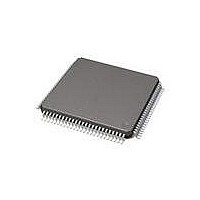
71M6534-IGT/F Maxim Integrated Products, 71M6534-IGT/F Datasheet - Page 24

71M6534-IGT/F
Manufacturer Part Number
71M6534-IGT/F
Description
IC ENERY METER 3PH 128K 120-LQFP
Manufacturer
Maxim Integrated Products
Datasheet
1.71M6533H-IGTF.pdf
(132 pages)
Specifications of 71M6534-IGT/F
Mounting Style
SMD/SMT
Package / Case
LQFP-120
Lead Free Status / RoHS Status
Lead free / RoHS Compliant
Available stocks
Company
Part Number
Manufacturer
Quantity
Price
Company:
Part Number:
71M6534-IGT/F
Manufacturer:
HONEYWELL
Quantity:
10
Company:
Part Number:
71M6534-IGT/F
Manufacturer:
Maxim Integrated
Quantity:
10 000
Part Number:
71M6534-IGT/F
Manufacturer:
MAXIM/美信
Quantity:
20 000
PUSH and CALL instructions, causing the stack to begin at location 0x08.
driver and an input buffer, therefore the MPU can output or read data through any of these ports. Even if
a DIO pin is configured as an output, the state of the pin can still be read by the MPU, for example when
counting pulses issued via DIO pins that are under CE control.
Clock Stretching (CKCON[2:0], SFR 0x8E)
Stack Pointer (SP, SFR 0x81):
The stack pointer is a 1-byte register initialized to 0x07 after reset. This register is incremented before
Data Pointer:
The data pointers (DPTR and DPRT1) are 2 bytes wide. The lower part is DPL(SFR 0x82) and DPL1 (SFR
0x84) and the highest is DPH (SFR 0x83) and DPH1 (SFR 0x85). The data pointers can be loaded as two
registers (e.g. MOV DPL,#data8). They are generally used to access external code or data space (e.g.
MOVC A,@A+DPTR or MOVX A,@DPTR respectively).
Program Counter:
The program counter (PC) is 2 bytes wide and initialized to 0x0000 after reset. The PC is incremented
when fetching operation code or when operating on data from program memory.
Port Registers:
The I/O ports are controlled by Special Function Registers P0, P1 and P2, as shown in
of the SFR can be observed on corresponding pins on the chip. Writing a 1 to any of the ports causes the
corresponding pin to be at high level (V3P3). Writing a 0 causes the corresponding pin to be held at a low
level (GND). The data direction registers DIR0, DIR1, and DIR2 define individual pins as input or output
pins (see
All DIO ports on the chip are bi-directional. Each of them consists of a Latch (SFR P0 to P2), an output
The CKCON[2:0] field defines the stretch memory cycles that are used for MOVX instructions when
accessing external peripherals. The practical value of this field for the 71M6533/71M6534 is to guarantee
access to XRAM between CE, MPU, and SPI. The default setting of CKCON[2:0] (001) should not be
changed.
Table 13
from 0 to 7. The widths of the signals are counted in MPU clock cycles. The post-reset state of the
CKCON[2:0] register (001), which is shown in bold in the table, performs the MOVX instructions with a
stretch value equal to 1.
24
P0
DIR0
P1
DIR1
P2
DIR2
Register
The technique of reading the status of or generating interrupts based on DIO pins configured as
outputs can be used to implement pulse counting.
shows how the signals of the External Memory Interface change when stretch values are set
Section
0x80
0xA2
0x90
0x91
0xA0
0xA1
Address
SFR
1.5.7 Digital I/O
R/W
R/W
R/W
R/W
R/W
R/W
R/W Description
Register for port 0 read and write operations.
Data direction register for port 0. Setting a bit to 1 means that the
corresponding pin is an output.
Register for port 1 read and write operations.
Data direction register for port 1.
Register for port 2 read and write operations.
Data direction register for port 2.
for details).
Table 12: Port Registers
Table
12. The contents
Rev 2


