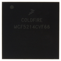
MCF5214CVF66 Freescale Semiconductor, MCF5214CVF66 Datasheet - Page 692

MCF5214CVF66
Manufacturer Part Number
MCF5214CVF66
Description
IC MPU 32BIT COLDF 256-MAPBGA
Manufacturer
Freescale Semiconductor
Series
MCF521xr
Datasheet
1.MCF5216CVM66J.pdf
(766 pages)
Specifications of MCF5214CVF66
Core Processor
Coldfire V2
Core Size
32-Bit
Speed
66MHz
Connectivity
CAN, EBI/EMI, I²C, SPI, UART/USART
Peripherals
DMA, LVD, POR, PWM, WDT
Number Of I /o
142
Program Memory Size
256KB (256K x 8)
Program Memory Type
FLASH
Ram Size
64K x 8
Voltage - Supply (vcc/vdd)
2.7 V ~ 3.6 V
Data Converters
A/D 8x12b
Oscillator Type
Internal
Operating Temperature
-40°C ~ 85°C
Package / Case
256-MAPBGA
Package
256MA-BGA
Device Core
ColdFire
Family Name
MCF521x
Maximum Speed
66 MHz
Operating Supply Voltage
3.3 V
Data Bus Width
32 Bit
Number Of Programmable I/os
142
Interface Type
QSPI/UART/I2C/CAN
On-chip Adc
8-chx10-bit
Number Of Timers
8
Lead Free Status / RoHS Status
Contains lead / RoHS non-compliant
Eeprom Size
-
Available stocks
Company
Part Number
Manufacturer
Quantity
Price
Company:
Part Number:
MCF5214CVF66
Manufacturer:
Freescale Semiconductor
Quantity:
10 000
Company:
Part Number:
MCF5214CVF66J
Manufacturer:
Freescale Semiconductor
Quantity:
10 000
- Current page: 692 of 766
- Download datasheet (9Mb)
Electrical Characteristics
33.6
33-8
6
7
8
9
10
11
1
2
3
4
5
6
Analog Supply, with reference to V
Internal Digital Supply
Reference Supply, with reference to V
V
V
V
V
V
V
Maximum Input Current
Load Capacitance determined from crystal manufacturer specifications and will include circuit board parasitics.
This specification applies to the period required for the PLL to relock after changing the MFD frequency control bits in the
synthesizer control register (SYNCR).
Assuming a reference is available at power up, lock time is measured from the time V
RSTO negating. If the crystal oscillator is being used as the reference for the PLL, then the crystal start up time
must be added to the PLL lock time to determine the total start-up time.
PLL is operating in 1:1 PLL mode.
Jitter is the average deviation from the programmed frequency measured over the specified interval at maximum f
Measurements are made with the device powered by filtered supplies and clocked by a stable external clock signal.
Noise injected into the PLL circuitry via V
Cjitter percentage for a given interval
Based on slow system clock of 40 MHz measured at f
SS
DD
REF
RH
RL
DDH
For internal digital supply of V
Refers to allowed random sequencing of power supplies.
Refers to allowed random sequencing of power supplies.
Transitions within the limit do not affect device reliability or cause permanent damage. Exceeding limit may cause
permanent conversion error on stressed channels and on unstressed channels.
Input must be current limited to the value specified. To determine the value of the required current-limiting resistor,
calculate resistance values using V
calculated values.
Condition applies to one pin at a time.
Differential Voltage
to V
Differential Voltage
to V
Differential Voltage
to V
QADC Electrical Characteristics
SSA
DDA
DDA
Differential Voltage
Differential Voltage
Differential Voltage
Parameter
1
, with reference to V
2
4, 5, 6
MCF5282 and MCF5216 ColdFire Microcontroller User’s Manual, Rev. 3
DD
Table 33-9. QADC Absolute Maximum Ratings
3
SSA
= 3.3V typical.
POSCLAMP
RL
DDPLL
SS
= V
and V
DDA
SSPLL
sys
+ 0.3V and V
V
V
V
V
V
V
DDH
max.
DD
RH
SS
Symbol
RL
RH
V
and variation in crystal oscillator frequency increase the
V
V
I
– V
– V
– V
– V
DDA
MA
DD
RH
– V
– V
SSA
DDA
DDA
SSA
RL
DDA
NEGCLAMP
–0.3
–0.3
–0.3
–0.1
–6.0
–0.3
–6.0
–0.3
–1.0
Min
–25
= –0.3 V, then use the larger of the
DD
and V
Max
6.0
4.0
6.0
0.1
4.0
6.0
6.0
0.3
1.0
25
DDPLL
Freescale Semiconductor
are valid to
Unit
mA
V
V
V
V
V
V
V
V
V
sys
.
Related parts for MCF5214CVF66
Image
Part Number
Description
Manufacturer
Datasheet
Request
R
Part Number:
Description:
Manufacturer:
Freescale Semiconductor, Inc
Datasheet:
Part Number:
Description:
Manufacturer:
Freescale Semiconductor, Inc
Datasheet:
Part Number:
Description:
Manufacturer:
Freescale Semiconductor, Inc
Datasheet:
Part Number:
Description:
Manufacturer:
Freescale Semiconductor, Inc
Datasheet:
Part Number:
Description:
Manufacturer:
Freescale Semiconductor, Inc
Datasheet:
Part Number:
Description:
Manufacturer:
Freescale Semiconductor, Inc
Datasheet:
Part Number:
Description:
Manufacturer:
Freescale Semiconductor, Inc
Datasheet:
Part Number:
Description:
Manufacturer:
Freescale Semiconductor, Inc
Datasheet:
Part Number:
Description:
Manufacturer:
Freescale Semiconductor, Inc
Datasheet:
Part Number:
Description:
Manufacturer:
Freescale Semiconductor, Inc
Datasheet:
Part Number:
Description:
Manufacturer:
Freescale Semiconductor, Inc
Datasheet:
Part Number:
Description:
Manufacturer:
Freescale Semiconductor, Inc
Datasheet:
Part Number:
Description:
Manufacturer:
Freescale Semiconductor, Inc
Datasheet:
Part Number:
Description:
Manufacturer:
Freescale Semiconductor, Inc
Datasheet:
Part Number:
Description:
Manufacturer:
Freescale Semiconductor, Inc
Datasheet:


