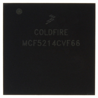
MCF5214CVF66 Freescale Semiconductor, MCF5214CVF66 Datasheet - Page 269

MCF5214CVF66
Manufacturer Part Number
MCF5214CVF66
Description
IC MPU 32BIT COLDF 256-MAPBGA
Manufacturer
Freescale Semiconductor
Series
MCF521xr
Datasheet
1.MCF5216CVM66J.pdf
(766 pages)
Specifications of MCF5214CVF66
Core Processor
Coldfire V2
Core Size
32-Bit
Speed
66MHz
Connectivity
CAN, EBI/EMI, I²C, SPI, UART/USART
Peripherals
DMA, LVD, POR, PWM, WDT
Number Of I /o
142
Program Memory Size
256KB (256K x 8)
Program Memory Type
FLASH
Ram Size
64K x 8
Voltage - Supply (vcc/vdd)
2.7 V ~ 3.6 V
Data Converters
A/D 8x12b
Oscillator Type
Internal
Operating Temperature
-40°C ~ 85°C
Package / Case
256-MAPBGA
Package
256MA-BGA
Device Core
ColdFire
Family Name
MCF521x
Maximum Speed
66 MHz
Operating Supply Voltage
3.3 V
Data Bus Width
32 Bit
Number Of Programmable I/os
142
Interface Type
QSPI/UART/I2C/CAN
On-chip Adc
8-chx10-bit
Number Of Timers
8
Lead Free Status / RoHS Status
Contains lead / RoHS non-compliant
Eeprom Size
-
Available stocks
Company
Part Number
Manufacturer
Quantity
Price
Company:
Part Number:
MCF5214CVF66
Manufacturer:
Freescale Semiconductor
Quantity:
10 000
Company:
Part Number:
MCF5214CVF66J
Manufacturer:
Freescale Semiconductor
Quantity:
10 000
- Current page: 269 of 766
- Download datasheet (9Mb)
Signal Descriptions
14.2.13.3 QADC Analog Input (AN2/ANY)
This PQB signal is the direct analog input AN2. When using external multiplexing this pin can also be
configured as multiplexed input ANY.
This pin can also be configured as GPIO PQB2.
14.2.13.4 QADC Analog Input (AN3/ANZ)
This PQB signal is the direct analog input AN3. When using external multiplexing this pin can also be
configured as multiplexed input ANZ.
This pin can also be configured as GPIO PQB3.
14.2.13.5 QADC Analog Input (AN52/MA0)
This PQA signal is the direct analog input AN52. When using external multiplexing this pin can also be
configured as an output signal, MA0, to select the output of the external multiplexer.
This pin can also be configured as GPIO PQA0.
14.2.13.6 QADC Analog Input (AN53/MA1)
This PQA signal is the direct analog input AN53. When using external multiplexing this pin can also be
configured as an output signal, MA1, to select the output of the external multiplexer.
This pin can also be configured as GPIO PQA1.
14.2.13.7 QADC Analog Input (AN55/TRIG1)
This PQA signal is the direct analog input AN55. This pin can also be configured as an input signal,
TRIG1, to trigger the execution of one of the two queues.
This pin can also be configured as GPIO PQA3.
14.2.13.8 QADC Analog Input (AN56/TRIG2)
This PQA signal is the direct analog input AN56. This pin can also be configured as an input signal,
TRIG2, to trigger the execution of one of the two queues.
This pin can also be configured as GPIO PQA4.
14.2.14 Debug Support Signals
These signals are used as the interface to the on-chip JTAG controller and also to interface to the BDM
logic.
14.2.14.1 JTAG_EN
This input signal is used to select between multiplexed debug module and JTAG signals at reset. If
JTAG_EN is low, the part is in normal and background debug mode (BDM); if it is high, it is in normal
and JTAG mode.
MCF5282 and MCF5216 ColdFire Microcontroller User’s Manual, Rev. 3
Freescale Semiconductor
14-29
Related parts for MCF5214CVF66
Image
Part Number
Description
Manufacturer
Datasheet
Request
R
Part Number:
Description:
Manufacturer:
Freescale Semiconductor, Inc
Datasheet:
Part Number:
Description:
Manufacturer:
Freescale Semiconductor, Inc
Datasheet:
Part Number:
Description:
Manufacturer:
Freescale Semiconductor, Inc
Datasheet:
Part Number:
Description:
Manufacturer:
Freescale Semiconductor, Inc
Datasheet:
Part Number:
Description:
Manufacturer:
Freescale Semiconductor, Inc
Datasheet:
Part Number:
Description:
Manufacturer:
Freescale Semiconductor, Inc
Datasheet:
Part Number:
Description:
Manufacturer:
Freescale Semiconductor, Inc
Datasheet:
Part Number:
Description:
Manufacturer:
Freescale Semiconductor, Inc
Datasheet:
Part Number:
Description:
Manufacturer:
Freescale Semiconductor, Inc
Datasheet:
Part Number:
Description:
Manufacturer:
Freescale Semiconductor, Inc
Datasheet:
Part Number:
Description:
Manufacturer:
Freescale Semiconductor, Inc
Datasheet:
Part Number:
Description:
Manufacturer:
Freescale Semiconductor, Inc
Datasheet:
Part Number:
Description:
Manufacturer:
Freescale Semiconductor, Inc
Datasheet:
Part Number:
Description:
Manufacturer:
Freescale Semiconductor, Inc
Datasheet:
Part Number:
Description:
Manufacturer:
Freescale Semiconductor, Inc
Datasheet:


