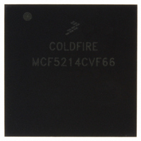
MCF5214CVF66 Freescale Semiconductor, MCF5214CVF66 Datasheet - Page 246

MCF5214CVF66
Manufacturer Part Number
MCF5214CVF66
Description
IC MPU 32BIT COLDF 256-MAPBGA
Manufacturer
Freescale Semiconductor
Series
MCF521xr
Datasheet
1.MCF5216CVM66J.pdf
(766 pages)
Specifications of MCF5214CVF66
Core Processor
Coldfire V2
Core Size
32-Bit
Speed
66MHz
Connectivity
CAN, EBI/EMI, I²C, SPI, UART/USART
Peripherals
DMA, LVD, POR, PWM, WDT
Number Of I /o
142
Program Memory Size
256KB (256K x 8)
Program Memory Type
FLASH
Ram Size
64K x 8
Voltage - Supply (vcc/vdd)
2.7 V ~ 3.6 V
Data Converters
A/D 8x12b
Oscillator Type
Internal
Operating Temperature
-40°C ~ 85°C
Package / Case
256-MAPBGA
Package
256MA-BGA
Device Core
ColdFire
Family Name
MCF521x
Maximum Speed
66 MHz
Operating Supply Voltage
3.3 V
Data Bus Width
32 Bit
Number Of Programmable I/os
142
Interface Type
QSPI/UART/I2C/CAN
On-chip Adc
8-chx10-bit
Number Of Timers
8
Lead Free Status / RoHS Status
Contains lead / RoHS non-compliant
Eeprom Size
-
Available stocks
Company
Part Number
Manufacturer
Quantity
Price
Company:
Part Number:
MCF5214CVF66
Manufacturer:
Freescale Semiconductor
Quantity:
10 000
Company:
Part Number:
MCF5214CVF66J
Manufacturer:
Freescale Semiconductor
Quantity:
10 000
- Current page: 246 of 766
- Download datasheet (9Mb)
Signal Descriptions
14-6
Clear-to-send
Request to send
GPTA
GPTB
External clock input
DMA timer input
DMA timer output
QADC analog input
QADC analog input
QADC analog input
JTAG_EN
Development serial
clock/Test reset
Breakpoint/
Test mode select
Signal Name
MCF5282 and MCF5216 ColdFire Microcontroller User’s Manual, Rev. 3
Table 14-1. MCF5282 Signal Description (continued)
UCTS[1:0]
URTS[1:0]
GPTA[3:0]
GPTB[3:0]
SYNCA/SYNCB
DTIN[3:0]
DTOUT[3:0]
AN[0:3]/AN[W:Z]
AN[52:53]/MA[0:1] Direct analog input ANn, or
AN[55:56]/
TRIG[1:2]
JTAG_EN
DSCLK/TRST
BKPT/TMS
Abbreviation
Analog-to-Digital Converter (QADC) Signals
General Purpose Timer Signals
Debug Support Signals
DMA Timer Signals
transmission.
Automatic UART request to send
outputs.
Provide the external interface to the
timer A functions.
Provide the external interface to the
timer B functions.
Clear the timer’s clock, providing a
means of synchronization to externally
clocked or timed events.
Clock the event counter or provide a
trigger to timer value capture logic.
Direct analog input ANn, or
multiplexed input ANx.
multiplexed output MAn. MAn selects
the output of the external multiplexer.
Direct analog input ANn, or input
TRIGn. TRIGn causes one of the two
queues to execute.
Selects between multiplexed debug
module and JTAG signals at reset.
Development serial clock for the serial
interface to debug module (DSCLK).
Asynchronously resets the internal
JTAG controller to the test logic reset
state (TRST).
Signals a hardware breakpoint in
debug mode (BKPT). Provides
information that determines JTAG test
operation mode (TMS).
Signals UART that it can begin data
Pulse or toggle on timer events.
Function
I/O
I/O
I/O
I/O
I/O
I/O
O
I
I
I
I
I
I
I
Freescale Semiconductor
14-26
14-27
14-27
14-27
14-27
14-27
14-27
14-28
14-29
14-29
14-29
14-30
14-30
Page
Related parts for MCF5214CVF66
Image
Part Number
Description
Manufacturer
Datasheet
Request
R
Part Number:
Description:
Manufacturer:
Freescale Semiconductor, Inc
Datasheet:
Part Number:
Description:
Manufacturer:
Freescale Semiconductor, Inc
Datasheet:
Part Number:
Description:
Manufacturer:
Freescale Semiconductor, Inc
Datasheet:
Part Number:
Description:
Manufacturer:
Freescale Semiconductor, Inc
Datasheet:
Part Number:
Description:
Manufacturer:
Freescale Semiconductor, Inc
Datasheet:
Part Number:
Description:
Manufacturer:
Freescale Semiconductor, Inc
Datasheet:
Part Number:
Description:
Manufacturer:
Freescale Semiconductor, Inc
Datasheet:
Part Number:
Description:
Manufacturer:
Freescale Semiconductor, Inc
Datasheet:
Part Number:
Description:
Manufacturer:
Freescale Semiconductor, Inc
Datasheet:
Part Number:
Description:
Manufacturer:
Freescale Semiconductor, Inc
Datasheet:
Part Number:
Description:
Manufacturer:
Freescale Semiconductor, Inc
Datasheet:
Part Number:
Description:
Manufacturer:
Freescale Semiconductor, Inc
Datasheet:
Part Number:
Description:
Manufacturer:
Freescale Semiconductor, Inc
Datasheet:
Part Number:
Description:
Manufacturer:
Freescale Semiconductor, Inc
Datasheet:
Part Number:
Description:
Manufacturer:
Freescale Semiconductor, Inc
Datasheet:


