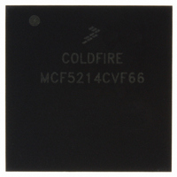
MCF5214CVF66 Freescale Semiconductor, MCF5214CVF66 Datasheet - Page 114

MCF5214CVF66
Manufacturer Part Number
MCF5214CVF66
Description
IC MPU 32BIT COLDF 256-MAPBGA
Manufacturer
Freescale Semiconductor
Series
MCF521xr
Datasheet
1.MCF5216CVM66J.pdf
(766 pages)
Specifications of MCF5214CVF66
Core Processor
Coldfire V2
Core Size
32-Bit
Speed
66MHz
Connectivity
CAN, EBI/EMI, I²C, SPI, UART/USART
Peripherals
DMA, LVD, POR, PWM, WDT
Number Of I /o
142
Program Memory Size
256KB (256K x 8)
Program Memory Type
FLASH
Ram Size
64K x 8
Voltage - Supply (vcc/vdd)
2.7 V ~ 3.6 V
Data Converters
A/D 8x12b
Oscillator Type
Internal
Operating Temperature
-40°C ~ 85°C
Package / Case
256-MAPBGA
Package
256MA-BGA
Device Core
ColdFire
Family Name
MCF521x
Maximum Speed
66 MHz
Operating Supply Voltage
3.3 V
Data Bus Width
32 Bit
Number Of Programmable I/os
142
Interface Type
QSPI/UART/I2C/CAN
On-chip Adc
8-chx10-bit
Number Of Timers
8
Lead Free Status / RoHS Status
Contains lead / RoHS non-compliant
Eeprom Size
-
Available stocks
Company
Part Number
Manufacturer
Quantity
Price
Company:
Part Number:
MCF5214CVF66
Manufacturer:
Freescale Semiconductor
Quantity:
10 000
Company:
Part Number:
MCF5214CVF66J
Manufacturer:
Freescale Semiconductor
Quantity:
10 000
- Current page: 114 of 766
- Download datasheet (9Mb)
ColdFire Flash Module (CFM)
6.2
Block Diagram
The CFM module shown in
Figure 6-1
contains the Flash physical blocks, the ColdFire Flash bus and IP
bus interfaces, Flash interface, register blocks, and the BIST engine.
Each 128-Kbyte Flash physical block is arranged as two 32,768-word (16 bits) memory arrays. Each of
these memory arrays is designated as xH or xL, where x represents one of the four Flash physical blocks
(0–3) and H/L represents the high or low 16 bits of each longword of logical memory. Each of these words
may be read as either individual bytes or aligned words. Aligned longword access is provided by
concatenating the outputs of the each of the two memory arrays within the Flash physical block. Simple
reads of bytes, aligned words, and aligned longwords require two 66-MHz clock cycles, although the
processor’s Flash interface includes logic that reduces the effective access time through two-way longword
interleaving and speculative reads.
Flash physical blocks are interleaved on longword (4-byte) boundaries. Therefore, all Flash program,
erase, and verify commands operate on adjacent Flash physical blocks and are initiated with a single
aligned 32-bit write to the appropriate array location. Any other write operation will cause a cycle
termination transfer error. Page erase operates simultaneously on two interleaving erase pages in adjacent
Flash physical blocks. Each Flash physical block is organized as 1024 rows of 128 bytes with a single erase
page consisting of 8 rows (1024 bytes). Since page erase operates simultaneously on two interleaving and
adjacent physical Flash blocks, each erase row is comprised of four 16-bit entries in each of two memory
arrays within each of two Flash physical blocks. The first row of Flash is made up of 0H_0L_1H_1L [0]
through 0H_0L_1H_1L [31], where each [n] represents four 16-bit words from each memory array in each
of two physical blocks, for a total of 256 bytes. Since a single erase page consists of 8 rows of 256 bytes,
or 2048 bytes, the first erase page is physically located at 0H_0L_1H_1L [0] through 0H_0L_1H_1L
[255]. Mass erase operates simultaneously on two adjacent Flash physical blocks in their entirety and
erases a total of 256 Kbytes of Flash space. Therefore, it takes two mass erase operations, one on mass
erase block 0 and one on mass erase block 1, to erase the full 512K CFM Flash on the MCF5282 and
MCF5216.
An erased Flash bit reads 1 and a programmed Flash bit reads 0. The CFM features a sense amplifier
timeout (SATO) block that automatically reduces current consumption during reads at low system clock
frequencies.
MCF5282 and MCF5216 ColdFire Microcontroller User’s Manual, Rev. 3
6-2
Freescale Semiconductor
Related parts for MCF5214CVF66
Image
Part Number
Description
Manufacturer
Datasheet
Request
R
Part Number:
Description:
Manufacturer:
Freescale Semiconductor, Inc
Datasheet:
Part Number:
Description:
Manufacturer:
Freescale Semiconductor, Inc
Datasheet:
Part Number:
Description:
Manufacturer:
Freescale Semiconductor, Inc
Datasheet:
Part Number:
Description:
Manufacturer:
Freescale Semiconductor, Inc
Datasheet:
Part Number:
Description:
Manufacturer:
Freescale Semiconductor, Inc
Datasheet:
Part Number:
Description:
Manufacturer:
Freescale Semiconductor, Inc
Datasheet:
Part Number:
Description:
Manufacturer:
Freescale Semiconductor, Inc
Datasheet:
Part Number:
Description:
Manufacturer:
Freescale Semiconductor, Inc
Datasheet:
Part Number:
Description:
Manufacturer:
Freescale Semiconductor, Inc
Datasheet:
Part Number:
Description:
Manufacturer:
Freescale Semiconductor, Inc
Datasheet:
Part Number:
Description:
Manufacturer:
Freescale Semiconductor, Inc
Datasheet:
Part Number:
Description:
Manufacturer:
Freescale Semiconductor, Inc
Datasheet:
Part Number:
Description:
Manufacturer:
Freescale Semiconductor, Inc
Datasheet:
Part Number:
Description:
Manufacturer:
Freescale Semiconductor, Inc
Datasheet:
Part Number:
Description:
Manufacturer:
Freescale Semiconductor, Inc
Datasheet:


