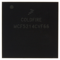
MCF5214CVF66 Freescale Semiconductor, MCF5214CVF66 Datasheet - Page 630

MCF5214CVF66
Manufacturer Part Number
MCF5214CVF66
Description
IC MPU 32BIT COLDF 256-MAPBGA
Manufacturer
Freescale Semiconductor
Series
MCF521xr
Datasheet
1.MCF5216CVM66J.pdf
(766 pages)
Specifications of MCF5214CVF66
Core Processor
Coldfire V2
Core Size
32-Bit
Speed
66MHz
Connectivity
CAN, EBI/EMI, I²C, SPI, UART/USART
Peripherals
DMA, LVD, POR, PWM, WDT
Number Of I /o
142
Program Memory Size
256KB (256K x 8)
Program Memory Type
FLASH
Ram Size
64K x 8
Voltage - Supply (vcc/vdd)
2.7 V ~ 3.6 V
Data Converters
A/D 8x12b
Oscillator Type
Internal
Operating Temperature
-40°C ~ 85°C
Package / Case
256-MAPBGA
Package
256MA-BGA
Device Core
ColdFire
Family Name
MCF521x
Maximum Speed
66 MHz
Operating Supply Voltage
3.3 V
Data Bus Width
32 Bit
Number Of Programmable I/os
142
Interface Type
QSPI/UART/I2C/CAN
On-chip Adc
8-chx10-bit
Number Of Timers
8
Lead Free Status / RoHS Status
Contains lead / RoHS non-compliant
Eeprom Size
-
Available stocks
Company
Part Number
Manufacturer
Quantity
Price
Company:
Part Number:
MCF5214CVF66
Manufacturer:
Freescale Semiconductor
Quantity:
10 000
Company:
Part Number:
MCF5214CVF66J
Manufacturer:
Freescale Semiconductor
Quantity:
10 000
- Current page: 630 of 766
- Download datasheet (9Mb)
Debug Support
30.4.5
The DBR, shown in
bits are masked by setting corresponding DBMR bits, as defined in TDR.
30-12
DRc[4–0]
9–8
3–0
Bit
7
6
5
4
Reset
Field
R/W DBR is accessible in supervisor mode as debug control register 0x0E, using the WDEBUG instruction and
Data Breakpoint/Mask Registers (DBR, DBMR)
Name
through the BDM port using the
DBMR is accessible in supervisor mode as debug control register 0x0F,using the WDEBUG instruction and
via the BDM port using the
SSM
BTB
NPL
IPI
—
—
31
Branch target bytes. Defines the number of bytes of branch target address DDATA displays.
00 0 bytes
01 Lower 2 bytes of the target address
10 Lower 3 bytes of the target address
11 Entire 4-byte target address
See
Reserved, should be cleared.
Non-pipelined mode. Determines whether the core operates in pipelined or mode or not.
0 Pipelined mode
1 Nonpipelined mode. The processor effectively executes one instruction at a time with no overlap.
Regardless of the NPL state, a triggered PC breakpoint is always reported before the triggering
instruction executes. In normal pipeline operation, the occurrence of an address and/or data
breakpoint trigger is imprecise. In non-pipeline mode, triggers are always reported before the next
instruction begins execution and trigger reporting can be considered precise.
Ignore pending interrupts.
1
0
Single-step mode. Setting SSM puts the processor in single-step mode.
0 Normal mode.
1 Single-step mode. The processor halts after execution of each instruction. While halted, any BDM
Reserved, should be cleared.
Figure
This adds at least 5 cycles to the execution time of each instruction. Given an average execution
latency of 1.6 cycles/instruction, throughput in non-pipeline mode would be 6.6 cycles/instruction,
approximately 25% or less of pipelined performance.
command can be executed. On receipt of the
instruction and halts again. This process continues until SSM is cleared.
Core ignores any pending interrupt requests signalled while in single-instruction-step mode.
Core services any pending interrupt requests that were signalled while in single-step mode.
Section 30.3.1, “Begin Execution of Taken Branch (PST =
Figure 30-8. Data Breakpoint/Mask Registers (DBR/DBMR)
MCF5282 and MCF5216 ColdFire Microcontroller User’s Manual, Rev. 3
30-8, specifies data patterns used as part of the trigger into debug mode. DBR
Table 30-8. CSR Field Descriptions (continued)
WDMREG
RDMREG
command.
Data (DBR); Mask (DBMR)
0x0E (DBR), 0x0F (DBMR)
and
WDMREG
Uninitialized
Description
commands.
GO
command, the processor executes the next
0x5).”
Freescale Semiconductor
0
Related parts for MCF5214CVF66
Image
Part Number
Description
Manufacturer
Datasheet
Request
R
Part Number:
Description:
Manufacturer:
Freescale Semiconductor, Inc
Datasheet:
Part Number:
Description:
Manufacturer:
Freescale Semiconductor, Inc
Datasheet:
Part Number:
Description:
Manufacturer:
Freescale Semiconductor, Inc
Datasheet:
Part Number:
Description:
Manufacturer:
Freescale Semiconductor, Inc
Datasheet:
Part Number:
Description:
Manufacturer:
Freescale Semiconductor, Inc
Datasheet:
Part Number:
Description:
Manufacturer:
Freescale Semiconductor, Inc
Datasheet:
Part Number:
Description:
Manufacturer:
Freescale Semiconductor, Inc
Datasheet:
Part Number:
Description:
Manufacturer:
Freescale Semiconductor, Inc
Datasheet:
Part Number:
Description:
Manufacturer:
Freescale Semiconductor, Inc
Datasheet:
Part Number:
Description:
Manufacturer:
Freescale Semiconductor, Inc
Datasheet:
Part Number:
Description:
Manufacturer:
Freescale Semiconductor, Inc
Datasheet:
Part Number:
Description:
Manufacturer:
Freescale Semiconductor, Inc
Datasheet:
Part Number:
Description:
Manufacturer:
Freescale Semiconductor, Inc
Datasheet:
Part Number:
Description:
Manufacturer:
Freescale Semiconductor, Inc
Datasheet:
Part Number:
Description:
Manufacturer:
Freescale Semiconductor, Inc
Datasheet:


