MC908MR32CFUE Freescale Semiconductor, MC908MR32CFUE Datasheet - Page 41
MC908MR32CFUE
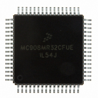
Manufacturer Part Number
MC908MR32CFUE
Description
IC MCU 8MHZ 32K FLASH 64-QFP
Manufacturer
Freescale Semiconductor
Series
HC08r
Datasheet
1.MC908MR16CFUE.pdf
(282 pages)
Specifications of MC908MR32CFUE
Core Processor
HC08
Core Size
8-Bit
Speed
8MHz
Connectivity
SCI, SPI
Peripherals
LVD, POR, PWM
Number Of I /o
44
Program Memory Size
32KB (32K x 8)
Program Memory Type
FLASH
Ram Size
768 x 8
Voltage - Supply (vcc/vdd)
4.5 V ~ 5.5 V
Data Converters
A/D 10x10b
Oscillator Type
Internal
Operating Temperature
-40°C ~ 85°C
Package / Case
64-QFP
Processor Series
HC08MR
Core
HC08
Data Bus Width
8 bit
Data Ram Size
768 B
Interface Type
SCI/SPI
Maximum Clock Frequency
8.2 MHz
Number Of Programmable I/os
44
Number Of Timers
6
Operating Supply Voltage
0 V to 5 V
Maximum Operating Temperature
+ 85 C
Mounting Style
SMD/SMT
Development Tools By Supplier
FSICEBASE, M68CBL05CE
Minimum Operating Temperature
- 40 C
On-chip Adc
10-ch x 10-bit
Lead Free Status / RoHS Status
Lead free / RoHS Compliant
Eeprom Size
-
Lead Free Status / Rohs Status
Lead free / RoHS Compliant
Available stocks
Company
Part Number
Manufacturer
Quantity
Price

Company:
Part Number:
MC908MR32CFUE
Manufacturer:
Freescale Semiconductor
Quantity:
10 000
Part Number:
MC908MR32CFUE
Manufacturer:
NXP/恩智浦
Quantity:
20 000


2.8.4 FLASH Program Operation
Use the following step-by-step procedure to program a row of FLASH memory.
flowchart of the programming algorithm.
This program sequence is repeated throughout the memory until all data is programmed.
1. The time between each FLASH address change, or the time between the last FLASH address programmed to clearing PGM
Freescale Semiconductor
10. Clear the PGM bit
11. Wait for time, t
12. Clear the HVEN bit.
13. After time, t
bit, must not exceed the maximum programming time, t
1. Set the PGM bit. This configures the memory for program operation and enables the latching of
2. Read the FLASH block protect register.
3. Write any data to any FLASH location within the address range desired.
4. Wait for a time, t
5. Set the HVEN bit.
6. Wait for a time, t
7. Write data to the FLASH address being programmed
8. Wait for time, t
9. Repeat step 7 and 8 until all desired bytes within the row are programmed.
address and data for programming.
Only bytes which are currently $FF may be programmed.
The COP register at location $FFFF should not be written between steps
5-12, when the HVEN bit is set. Since this register is located at a valid
FLASH address, unpredictable behavior may occur if this location is written
while HVEN is set.
Programming and erasing of FLASH locations cannot be performed by
code being executed from the FLASH memory. While these operations
must be performed in the order shown, other unrelated operations may
occur between the steps. Do not exceed t
Memory
RCV
PROG
NVH
(typical 1 µs), the memory can be accessed in read mode again.
NVS
PGS
Characteristics.
(1)
(minimum 5 µs).
MC68HC908MR32 • MC68HC908MR16 Data Sheet, Rev. 6.1
.
(minimum 30 µs).
(minimum 10 µs).
(minimum 5 µs).
PROG
NOTE
NOTE
NOTE
maximum.
PROG
(1)
maximum, see
.
19.6 FLASH
Figure 2-4
FLASH Memory (FLASH)
shows a
41
Related parts for MC908MR32CFUE
Image
Part Number
Description
Manufacturer
Datasheet
Request
R

Part Number:
Description:
Manufacturer:
Freescale Semiconductor, Inc
Datasheet:
Part Number:
Description:
Manufacturer:
Freescale Semiconductor, Inc
Datasheet:
Part Number:
Description:
Manufacturer:
Freescale Semiconductor, Inc
Datasheet:
Part Number:
Description:
Manufacturer:
Freescale Semiconductor, Inc
Datasheet:
Part Number:
Description:
Manufacturer:
Freescale Semiconductor, Inc
Datasheet:
Part Number:
Description:
Manufacturer:
Freescale Semiconductor, Inc
Datasheet:
Part Number:
Description:
Manufacturer:
Freescale Semiconductor, Inc
Datasheet:
Part Number:
Description:
Manufacturer:
Freescale Semiconductor, Inc
Datasheet:
Part Number:
Description:
Manufacturer:
Freescale Semiconductor, Inc
Datasheet:
Part Number:
Description:
Manufacturer:
Freescale Semiconductor, Inc
Datasheet:
Part Number:
Description:
Manufacturer:
Freescale Semiconductor, Inc
Datasheet:
Part Number:
Description:
Manufacturer:
Freescale Semiconductor, Inc
Datasheet:
Part Number:
Description:
Manufacturer:
Freescale Semiconductor, Inc
Datasheet:
Part Number:
Description:
Manufacturer:
Freescale Semiconductor, Inc
Datasheet:
Part Number:
Description:
Manufacturer:
Freescale Semiconductor, Inc
Datasheet: