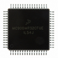
MC908MR32CFUE Freescale Semiconductor, MC908MR32CFUE Datasheet - Page 127

MC908MR32CFUE
Manufacturer Part Number
MC908MR32CFUE
Description
IC MCU 8MHZ 32K FLASH 64-QFP
Manufacturer
Freescale Semiconductor
Series
HC08r
Datasheet
1.MC908MR16CFUE.pdf
(282 pages)
Specifications of MC908MR32CFUE
Core Processor
HC08
Core Size
8-Bit
Speed
8MHz
Connectivity
SCI, SPI
Peripherals
LVD, POR, PWM
Number Of I /o
44
Program Memory Size
32KB (32K x 8)
Program Memory Type
FLASH
Ram Size
768 x 8
Voltage - Supply (vcc/vdd)
4.5 V ~ 5.5 V
Data Converters
A/D 10x10b
Oscillator Type
Internal
Operating Temperature
-40°C ~ 85°C
Package / Case
64-QFP
Processor Series
HC08MR
Core
HC08
Data Bus Width
8 bit
Data Ram Size
768 B
Interface Type
SCI/SPI
Maximum Clock Frequency
8.2 MHz
Number Of Programmable I/os
44
Number Of Timers
6
Operating Supply Voltage
0 V to 5 V
Maximum Operating Temperature
+ 85 C
Mounting Style
SMD/SMT
Development Tools By Supplier
FSICEBASE, M68CBL05CE
Minimum Operating Temperature
- 40 C
On-chip Adc
10-ch x 10-bit
Lead Free Status / RoHS Status
Lead free / RoHS Compliant
Eeprom Size
-
Lead Free Status / Rohs Status
Lead free / RoHS Compliant
Available stocks
Company
Part Number
Manufacturer
Quantity
Price
Company:
Part Number:
MC908MR32CFUE
Manufacturer:
Freescale Semiconductor
Quantity:
10 000
Part Number:
MC908MR32CFUE
Manufacturer:
NXP/恩智浦
Quantity:
20 000
- Current page: 127 of 282
- Download datasheet (2Mb)
When complementary operation is used, two additional features are provided:
If independent operation is chosen, each PWM has its own PWM value register.
12.5.2 Dead-Time Insertion
As shown in
top-side/bottom-side transistors.
When controlling dc-to-ac inverters such as this, the top and bottom PWMs in one pair should never be
active at the same time. In
would flow through the two transistors as they discharge the bus capacitor. The IGBTs could be
weakened or destroyed.
Simply forcing the two PWMs to be inversions of each other is not always sufficient. Since a time delay is
associated with turning off the transistors in the motor drive, there must be a dead-time between the
deactivation of one PWM and the activation of the other.
A dead-time can be specified in the dead-time write-once register. This 8-bit value specifies the number
of CPU clock cycles to use for the dead-time. The dead-time is not affected by changes in the PWM period
caused by the prescaler.
Dead-time insertion is achieved by feeding the top PWM outputs of the PWM generator into dead-time
generators, as shown in
pair to use for the top PWM in the next PWM cycle. See
Current Polarity
generator outputs, are fed into the dead-time generators. See
Whenever an input to a dead-time generator transitions, a dead-time is inserted (for example, both PWMs
in the pair are forced to their inactive state). The bottom PWM signal is generated from the top PWM and
the dead-time. In the case of output control enabled, the odd OUTx bits control the top PWMs, the even
OUTx bits control the bottom PWMs with respect to the odd OUTx bits (see
shows the effects of the dead-time insertion.
As seen in
pulse widths are reduced. For example, in
the ideal waveform (with no dead-time) has pulse widths equal to four. However, the actual pulse widths
shrink to two after a dead-time of two was inserted. In this example, with the prescaler set to divide by
one and center-aligned operation selected, this distortion can be compensated for by adding or
subtracting half the dead-time value to or from the PWM register value. This correction is further described
in
Further examples of dead-time insertion are shown in
the effects of dead-time insertion at the duty cycle boundaries (near 0 percent and 100 percent duty
cycles).
Freescale Semiconductor
12.5.3 Top/Bottom Correction with Motor Phase Current Polarity
•
•
Dead-time insertion
Separate top/bottom pulse width correction to correct for distortions caused by the motor drive
characteristics
Figure 12-17
Figure
Figure
Sensing. When output control is enabled, the odd OUT bits, rather than the PWM
12-15, some pulse width distortion occurs when the dead-time is inserted. The active
12-13, in complementary mode, each PWM pair can be used to drive
shows the effects of dead-time insertion on pulse widths smaller than the dead-time.
Figure
MC68HC908MR32 • MC68HC908MR16 Data Sheet, Rev. 6.1
Figure
12-14. Current sensing determines which PWM value of a PWM generator
12-13, if PWM1 and PWM2 were on at the same time, large currents
Figure
12-15, when the PWM value register is equal to two,
Figure 12-16
12.5.3 Top/Bottom Correction with Motor Phase
12.5.5 PWM Output Port
and
Sensing.
Figure
Table
12-17.
12-6).
Figure 12-16
Control.
Figure 12-15
Output Control
shows
127
Related parts for MC908MR32CFUE
Image
Part Number
Description
Manufacturer
Datasheet
Request
R
Part Number:
Description:
Manufacturer:
Freescale Semiconductor, Inc
Datasheet:
Part Number:
Description:
Manufacturer:
Freescale Semiconductor, Inc
Datasheet:
Part Number:
Description:
Manufacturer:
Freescale Semiconductor, Inc
Datasheet:
Part Number:
Description:
Manufacturer:
Freescale Semiconductor, Inc
Datasheet:
Part Number:
Description:
Manufacturer:
Freescale Semiconductor, Inc
Datasheet:
Part Number:
Description:
Manufacturer:
Freescale Semiconductor, Inc
Datasheet:
Part Number:
Description:
Manufacturer:
Freescale Semiconductor, Inc
Datasheet:
Part Number:
Description:
Manufacturer:
Freescale Semiconductor, Inc
Datasheet:
Part Number:
Description:
Manufacturer:
Freescale Semiconductor, Inc
Datasheet:
Part Number:
Description:
Manufacturer:
Freescale Semiconductor, Inc
Datasheet:
Part Number:
Description:
Manufacturer:
Freescale Semiconductor, Inc
Datasheet:
Part Number:
Description:
Manufacturer:
Freescale Semiconductor, Inc
Datasheet:
Part Number:
Description:
Manufacturer:
Freescale Semiconductor, Inc
Datasheet:
Part Number:
Description:
Manufacturer:
Freescale Semiconductor, Inc
Datasheet:
Part Number:
Description:
Manufacturer:
Freescale Semiconductor, Inc
Datasheet:


