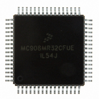
MC908MR32CFUE Freescale Semiconductor, MC908MR32CFUE Datasheet - Page 154

MC908MR32CFUE
Manufacturer Part Number
MC908MR32CFUE
Description
IC MCU 8MHZ 32K FLASH 64-QFP
Manufacturer
Freescale Semiconductor
Series
HC08r
Datasheet
1.MC908MR16CFUE.pdf
(282 pages)
Specifications of MC908MR32CFUE
Core Processor
HC08
Core Size
8-Bit
Speed
8MHz
Connectivity
SCI, SPI
Peripherals
LVD, POR, PWM
Number Of I /o
44
Program Memory Size
32KB (32K x 8)
Program Memory Type
FLASH
Ram Size
768 x 8
Voltage - Supply (vcc/vdd)
4.5 V ~ 5.5 V
Data Converters
A/D 10x10b
Oscillator Type
Internal
Operating Temperature
-40°C ~ 85°C
Package / Case
64-QFP
Processor Series
HC08MR
Core
HC08
Data Bus Width
8 bit
Data Ram Size
768 B
Interface Type
SCI/SPI
Maximum Clock Frequency
8.2 MHz
Number Of Programmable I/os
44
Number Of Timers
6
Operating Supply Voltage
0 V to 5 V
Maximum Operating Temperature
+ 85 C
Mounting Style
SMD/SMT
Development Tools By Supplier
FSICEBASE, M68CBL05CE
Minimum Operating Temperature
- 40 C
On-chip Adc
10-ch x 10-bit
Lead Free Status / RoHS Status
Lead free / RoHS Compliant
Eeprom Size
-
Lead Free Status / Rohs Status
Lead free / RoHS Compliant
Available stocks
Company
Part Number
Manufacturer
Quantity
Price
Company:
Part Number:
MC908MR32CFUE
Manufacturer:
Freescale Semiconductor
Quantity:
10 000
Part Number:
MC908MR32CFUE
Manufacturer:
NXP/恩智浦
Quantity:
20 000
- Current page: 154 of 282
- Download datasheet (2Mb)
Pulse-Width Modulator for Motor Control (PWMMC)
DT2 — Dead-Time 2 Bit
DT1 — Dead-Time 1 Bit
12.9.11 PWM Output Control Register
The PWM output control register (PWMOUT) is used to manually control the PWM pins.
OUTCTL— Output Control Enable Bit
OUT6–OUT1— PWM Pin Output Control Bits
154
Current sensing pin IS1 is monitored immediately before dead-time ends due to the assertion of
PWM2.
Current sensing pin IS1 is monitored immediately before dead-time ends due to the assertion of
PWM1.
This read/write bit allows the user to manually control the PWM pins. When set, the PWM generator is
no longer the input to the dead-time and output circuitry. The OUTx bits determine the state of the
PWM pins. Setting the OUTCTL bit does not disable the PWM generator. The generator continues to
run, but is no longer the input to the PWM dead-time and output circuitry. When OUTCTL is cleared,
the outputs of the PWM generator immediately become the inputs to the dead-time and output circuitry.
These read/write bits control the PWM pins according to
1 = PWM outputs controlled manually
0 = PWM outputs determined by PWM generator
Address: $0025
Reset:
Read:
Write:
OUTx Bit
OUT1
OUT2
OUT3
OUT4
OUT5
OUT6
Figure 12-46. PWM Output Control Register (PWMOUT)
Bit 7
0
0
MC68HC908MR32 • MC68HC908MR16 Data Sheet, Rev. 6.1
1 — PWM1 is active.
0 — PWM1 is inactive.
1 — PWM2 is complement of PWM 1.
0 — PWM2 is inactive.
1 — PWM3 is active.
0 — PWM3 is inactive.
1 — PWM4 is complement of PWM 3.
0 — PWM4 is inactive.
1 — PWM5 is active.
0 — PWM5 is inactive.
1 — PWM 6 is complement of PWM 5.
0 — PWM6 is inactive.
= Unimplemented
OUTCTL
6
0
Complementary Mode
Table 12-10. OUTx Bits
OUT6
5
0
OUT5
4
0
OUT4
3
0
Table
12-10.
1 — PWM1 is active.
0 — PWM1 is inactive.
1 — PWM2 is active.
0 — PWM2 is inactive.
1 — PWM3 is active.
0 — PWM3 is inactive.
1 — PWM4 is active.
0 — PWM4 is inactive.
1 — PWM5 is active.
0 — PWM5 is inactive.
1 — PWM6 is active.
0 — PWM6 is inactive.
OUT3
2
0
Independent Mode
OUT2
1
0
Freescale Semiconductor
OUT1
Bit 0
0
Related parts for MC908MR32CFUE
Image
Part Number
Description
Manufacturer
Datasheet
Request
R
Part Number:
Description:
Manufacturer:
Freescale Semiconductor, Inc
Datasheet:
Part Number:
Description:
Manufacturer:
Freescale Semiconductor, Inc
Datasheet:
Part Number:
Description:
Manufacturer:
Freescale Semiconductor, Inc
Datasheet:
Part Number:
Description:
Manufacturer:
Freescale Semiconductor, Inc
Datasheet:
Part Number:
Description:
Manufacturer:
Freescale Semiconductor, Inc
Datasheet:
Part Number:
Description:
Manufacturer:
Freescale Semiconductor, Inc
Datasheet:
Part Number:
Description:
Manufacturer:
Freescale Semiconductor, Inc
Datasheet:
Part Number:
Description:
Manufacturer:
Freescale Semiconductor, Inc
Datasheet:
Part Number:
Description:
Manufacturer:
Freescale Semiconductor, Inc
Datasheet:
Part Number:
Description:
Manufacturer:
Freescale Semiconductor, Inc
Datasheet:
Part Number:
Description:
Manufacturer:
Freescale Semiconductor, Inc
Datasheet:
Part Number:
Description:
Manufacturer:
Freescale Semiconductor, Inc
Datasheet:
Part Number:
Description:
Manufacturer:
Freescale Semiconductor, Inc
Datasheet:
Part Number:
Description:
Manufacturer:
Freescale Semiconductor, Inc
Datasheet:
Part Number:
Description:
Manufacturer:
Freescale Semiconductor, Inc
Datasheet:


