MC908MR32CFUE Freescale Semiconductor, MC908MR32CFUE Datasheet - Page 181
MC908MR32CFUE
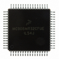
Manufacturer Part Number
MC908MR32CFUE
Description
IC MCU 8MHZ 32K FLASH 64-QFP
Manufacturer
Freescale Semiconductor
Series
HC08r
Datasheet
1.MC908MR16CFUE.pdf
(282 pages)
Specifications of MC908MR32CFUE
Core Processor
HC08
Core Size
8-Bit
Speed
8MHz
Connectivity
SCI, SPI
Peripherals
LVD, POR, PWM
Number Of I /o
44
Program Memory Size
32KB (32K x 8)
Program Memory Type
FLASH
Ram Size
768 x 8
Voltage - Supply (vcc/vdd)
4.5 V ~ 5.5 V
Data Converters
A/D 10x10b
Oscillator Type
Internal
Operating Temperature
-40°C ~ 85°C
Package / Case
64-QFP
Processor Series
HC08MR
Core
HC08
Data Bus Width
8 bit
Data Ram Size
768 B
Interface Type
SCI/SPI
Maximum Clock Frequency
8.2 MHz
Number Of Programmable I/os
44
Number Of Timers
6
Operating Supply Voltage
0 V to 5 V
Maximum Operating Temperature
+ 85 C
Mounting Style
SMD/SMT
Development Tools By Supplier
FSICEBASE, M68CBL05CE
Minimum Operating Temperature
- 40 C
On-chip Adc
10-ch x 10-bit
Lead Free Status / RoHS Status
Lead free / RoHS Compliant
Eeprom Size
-
Lead Free Status / Rohs Status
Lead free / RoHS Compliant
Available stocks
Company
Part Number
Manufacturer
Quantity
Price

Company:
Part Number:
MC908MR32CFUE
Manufacturer:
Freescale Semiconductor
Quantity:
10 000
Part Number:
MC908MR32CFUE
Manufacturer:
NXP/恩智浦
Quantity:
20 000


Chapter 14
System Integration Module (SIM)
14.1 Introduction
This section describes the system integration module (SIM). Together with the central processor unit
(CPU), the SIM controls all microcontroller unit (MCU) activities.
A block diagram of the SIM is shown in
The SIM is a system state controller that coordinates CPU and exception timing. The SIM is responsible
for:
Table 14-1
Freescale Semiconductor
Signal Name
•
•
•
•
•
CGMXCLK
CGMVCLK
CGMOUT
PORRST
IRST
R/W
IAB
IDB
Bus clock generation and control for CPU and peripherals:
–
–
Master reset control, including power-on reset (POR) and computer operating properly (COP)
timeout
Interrupt control:
–
–
–
CPU enable/disable timing
Modular architecture expandable to 128 interrupt sources
Wait/reset/break entry and recovery
Internal clock control
Acknowledge timing
Arbitration control timing
Vector address generation
shows the internal signal names used in this section.
Buffered version of OSC1 from clock generator module (CGM)
Phase-locked loop (PLL) circuit output
PLL-based or OSC1-based clock output from CGM module (bus clock = CGMOUT divided by two)
Internal address bus
Internal data bus
Internal reset signal
Read/write signal
Signal from the power-on reset module to the SIM
MC68HC908MR32 • MC68HC908MR16 Data Sheet, Rev. 6.1
Table 14-1. Signal Name Conventions
Figure
14-1.
Description
181
Related parts for MC908MR32CFUE
Image
Part Number
Description
Manufacturer
Datasheet
Request
R

Part Number:
Description:
Manufacturer:
Freescale Semiconductor, Inc
Datasheet:
Part Number:
Description:
Manufacturer:
Freescale Semiconductor, Inc
Datasheet:
Part Number:
Description:
Manufacturer:
Freescale Semiconductor, Inc
Datasheet:
Part Number:
Description:
Manufacturer:
Freescale Semiconductor, Inc
Datasheet:
Part Number:
Description:
Manufacturer:
Freescale Semiconductor, Inc
Datasheet:
Part Number:
Description:
Manufacturer:
Freescale Semiconductor, Inc
Datasheet:
Part Number:
Description:
Manufacturer:
Freescale Semiconductor, Inc
Datasheet:
Part Number:
Description:
Manufacturer:
Freescale Semiconductor, Inc
Datasheet:
Part Number:
Description:
Manufacturer:
Freescale Semiconductor, Inc
Datasheet:
Part Number:
Description:
Manufacturer:
Freescale Semiconductor, Inc
Datasheet:
Part Number:
Description:
Manufacturer:
Freescale Semiconductor, Inc
Datasheet:
Part Number:
Description:
Manufacturer:
Freescale Semiconductor, Inc
Datasheet:
Part Number:
Description:
Manufacturer:
Freescale Semiconductor, Inc
Datasheet:
Part Number:
Description:
Manufacturer:
Freescale Semiconductor, Inc
Datasheet:
Part Number:
Description:
Manufacturer:
Freescale Semiconductor, Inc
Datasheet: