MC908MR32CFUE Freescale Semiconductor, MC908MR32CFUE Datasheet - Page 229
MC908MR32CFUE
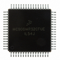
Manufacturer Part Number
MC908MR32CFUE
Description
IC MCU 8MHZ 32K FLASH 64-QFP
Manufacturer
Freescale Semiconductor
Series
HC08r
Datasheet
1.MC908MR16CFUE.pdf
(282 pages)
Specifications of MC908MR32CFUE
Core Processor
HC08
Core Size
8-Bit
Speed
8MHz
Connectivity
SCI, SPI
Peripherals
LVD, POR, PWM
Number Of I /o
44
Program Memory Size
32KB (32K x 8)
Program Memory Type
FLASH
Ram Size
768 x 8
Voltage - Supply (vcc/vdd)
4.5 V ~ 5.5 V
Data Converters
A/D 10x10b
Oscillator Type
Internal
Operating Temperature
-40°C ~ 85°C
Package / Case
64-QFP
Processor Series
HC08MR
Core
HC08
Data Bus Width
8 bit
Data Ram Size
768 B
Interface Type
SCI/SPI
Maximum Clock Frequency
8.2 MHz
Number Of Programmable I/os
44
Number Of Timers
6
Operating Supply Voltage
0 V to 5 V
Maximum Operating Temperature
+ 85 C
Mounting Style
SMD/SMT
Development Tools By Supplier
FSICEBASE, M68CBL05CE
Minimum Operating Temperature
- 40 C
On-chip Adc
10-ch x 10-bit
Lead Free Status / RoHS Status
Lead free / RoHS Compliant
Eeprom Size
-
Lead Free Status / Rohs Status
Lead free / RoHS Compliant
Available stocks
Company
Part Number
Manufacturer
Quantity
Price

Company:
Part Number:
MC908MR32CFUE
Manufacturer:
Freescale Semiconductor
Quantity:
10 000
Part Number:
MC908MR32CFUE
Manufacturer:
NXP/恩智浦
Quantity:
20 000


CHxF — Channel x Flag Bit
CHxIE — Channel x Interrupt Enable Bit
Freescale Semiconductor
When channel x is an input capture channel, this read/write bit is set when an active edge occurs on
the channel x pin. When channel x is an output compare channel, CHxF is set when the value in the
TIMA counter registers matches the value in the TIMA channel x registers.
When CHxIE = 1, clear CHxF by reading TIMA channel x status and control register with CHxF set,
and then writing a 0 to CHxF. If another interrupt request occurs before the clearing sequence is
complete, then writing 0 to CHxF has no effect. Therefore, an interrupt request cannot be lost due to
inadvertent clearing of CHxF.
Reset clears the CHxF bit. Writing a 1 to CHxF has no effect.
This read/write bit enables TIMA CPU interrupts on channel x.
Reset clears the CHxIE bit.
1 = Input capture or output compare on channel x
0 = No input capture or output compare on channel x
1 = Channel x CPU interrupt requests enabled
0 = Channel x CPU interrupt requests disabled
Register Name and Address:
Register Name and Address:
Register Name and Address:
Register Name and Address:
Reset:
Reset:
Reset:
Reset:
Read:
Read:
Read:
Read:
Write:
Write:
Write:
Write:
CH0F
CH1F
CH2F
CH3F
Bit 7
Bit 7
Bit 7
Bit 7
R
0
0
0
0
0
0
0
0
MC68HC908MR32 • MC68HC908MR16 Data Sheet, Rev. 6.1
= Reserved
and Control Registers (TASC0–TASC3)
CH0IE
CH1IE
CH2IE
CH3IE
6
0
6
0
6
0
6
0
Figure 16-8. TIMA Channel Status
TASC0 — $0013
TASC1 — $0016
TASC2 — $0019
TASC3 — $001C
MS0B
MS2B
R
R
5
0
5
0
0
5
0
5
0
0
MS0A
MS1A
MS2A
MS3A
4
0
4
0
4
0
4
0
ELS0B
ELS1B
ELS2B
ELS3B
3
0
3
0
3
0
3
0
ELS0A
ELS1A
ELS2A
ELS3A
2
0
2
0
2
0
2
0
TOV0
TOV1
TOV2
TOV3
1
0
1
0
1
0
1
0
CH0MAX
CH1MAX
CH2MAX
CH3MAX
Bit 0
Bit 0
Bit 0
Bit 0
0
0
0
0
I/O Registers
229
Related parts for MC908MR32CFUE
Image
Part Number
Description
Manufacturer
Datasheet
Request
R

Part Number:
Description:
Manufacturer:
Freescale Semiconductor, Inc
Datasheet:
Part Number:
Description:
Manufacturer:
Freescale Semiconductor, Inc
Datasheet:
Part Number:
Description:
Manufacturer:
Freescale Semiconductor, Inc
Datasheet:
Part Number:
Description:
Manufacturer:
Freescale Semiconductor, Inc
Datasheet:
Part Number:
Description:
Manufacturer:
Freescale Semiconductor, Inc
Datasheet:
Part Number:
Description:
Manufacturer:
Freescale Semiconductor, Inc
Datasheet:
Part Number:
Description:
Manufacturer:
Freescale Semiconductor, Inc
Datasheet:
Part Number:
Description:
Manufacturer:
Freescale Semiconductor, Inc
Datasheet:
Part Number:
Description:
Manufacturer:
Freescale Semiconductor, Inc
Datasheet:
Part Number:
Description:
Manufacturer:
Freescale Semiconductor, Inc
Datasheet:
Part Number:
Description:
Manufacturer:
Freescale Semiconductor, Inc
Datasheet:
Part Number:
Description:
Manufacturer:
Freescale Semiconductor, Inc
Datasheet:
Part Number:
Description:
Manufacturer:
Freescale Semiconductor, Inc
Datasheet:
Part Number:
Description:
Manufacturer:
Freescale Semiconductor, Inc
Datasheet:
Part Number:
Description:
Manufacturer:
Freescale Semiconductor, Inc
Datasheet: