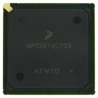
MPC561MZP56 Freescale Semiconductor, MPC561MZP56 Datasheet - Page 818

MPC561MZP56
Manufacturer Part Number
MPC561MZP56
Description
IC MPU 32BIT 56MHZ PPC 388-PBGA
Manufacturer
Freescale Semiconductor
Series
MPC5xxr
Datasheet
1.MPC561MZP56.pdf
(1420 pages)
Specifications of MPC561MZP56
Core Processor
PowerPC
Core Size
32-Bit
Speed
56MHz
Connectivity
CAN, EBI/EMI, SCI, SPI, UART/USART
Peripherals
POR, PWM, WDT
Number Of I /o
64
Program Memory Type
ROMless
Ram Size
32K x 8
Voltage - Supply (vcc/vdd)
2.5 V ~ 2.7 V
Data Converters
A/D 32x10b
Oscillator Type
External
Operating Temperature
-40°C ~ 125°C
Package / Case
388-BGA
Controller Family/series
POWER 5xx
No. Of I/o's
56
Ram Memory Size
31KB
Cpu Speed
56MHz
No. Of Timers
32
Embedded Interface Type
QSPI, SCI, UART
No. Of Pwm Channels
12
Rohs Compliant
No
Processor Series
MPC5xx
Core
PowerPC
Data Bus Width
32 bit
Data Ram Size
32 KB
Interface Type
CAN, JTAG, QSPI, SCI, SPI, UART
Maximum Clock Frequency
40 MHz
Number Of Programmable I/os
56
Number Of Timers
22
Operating Supply Voltage
2.6 V to 5 V
Maximum Operating Temperature
+ 85 C
Mounting Style
SMD/SMT
Minimum Operating Temperature
- 40 C
On-chip Adc
2 (10 bit, 32 Channel)
For Use With
MPC564EVB - KIT EVAL FOR MPC561/562/563/564
Lead Free Status / RoHS Status
Contains lead / RoHS non-compliant
Eeprom Size
-
Program Memory Size
-
Lead Free Status / Rohs Status
No
Available stocks
Company
Part Number
Manufacturer
Quantity
Price
Company:
Part Number:
MPC561MZP56
Manufacturer:
Freescale Semiconductor
Quantity:
10 000
Company:
Part Number:
MPC561MZP56R2
Manufacturer:
Freescale Semiconductor
Quantity:
10 000
- Current page: 818 of 1420
- Download datasheet (11Mb)
Peripheral Pin Multiplexing (PPM) Module
18.4.2
18-12
SRESET
Field SAMP[0:2] OP_16_8 ENRX ENTX
Addr
Bits
0:2
3
4
5
6
7
8
9
MSB
PPM Control Register (PPMPCR)
0
SAMP[0:2]
OP_16_8
1
ENRX
ENTX
Name
STR
SPI
CP
CI
2
2
1
3
The Sample rate is the rate at which the data registers are sampled, with respect to the
frequency of TCLK. For transmit, SAMP[0:2] is the rate at which data from the TX_DATA
register is sampled. For receive, SAMP[0:2] is the rate at which data is sampled from
RX_DATA.
Refer to
This bit describes how the 16 data bits will be transmitted and received. Both transmit and
receive are effected by this bit setting.
0 16 TCLK Cycles per word. All 16 bits of TX_DATA[0:15] will transmit on PPM_TX0. All 16
1 8 TCLK Cycles per word. TX_DATA[0:7] will transmit on PPM_TX1, TX_DATA[8:15] will
PPM Receive (RX) data enable.
0 RX Disabled
1 RX Enabled
PPM Transmit (TX) data enable.
0 TX Disabled
1 TX Enabled
SPI mode enable.
0 TDM mode enabled
1 SPI mode enabled
Start-Transmit-Receive bit. When this bit is set and SPI mode is enabled, the PPM module
will start to transmit and/or receive one frame of data. The STR bit will then be cleared
automatically by the PPM. Refer to
0 PPM has completed transmitting and/or receiving one data frame.
1 PPM will transmit and/or receive one data frame.
Clock Invert. This bit defines the polarity of TCLK clock in both SPI and TDM modes.
0 Normal clock polarity – active high clocks selected
1 Inverted clock – active low clocks selected
Clock Phase. This bit selects one of two fundamentally different transfer formats. Refer to
figures
0 Valid data can be latched on the transition of TCLK from inactive phase to active phase.
1 Valid data can be latched on the transition of TCLK from active phase to inactive phase.
bits of RX_SHIFTER[0:15] are received from PPM_RX0.
transmit on PPM_TX_0. RX_SHIFTER[0:7] are received from PPM_RX1,
RX_SHIFTER[8:15] are received from PPM_RX0.
Figure 18-9. PPM Control Register (PPMPCR)
MPC561/MPC563 Reference Manual, Rev. 1.2
Figure 18-12
Table 18-4
Table 18-3. PPMPCR Bit Descriptions
4
5
for SAMP[0:2] settings.
and
SPI
0000_0000_0000_0000
6
Figure
STR
0x30 5C04
7
18-13.
Table
CI
Description
8
18-5.
CP
9
CM
10
11
12
RESERVED
Freescale Semiconductor
13
14
LSB
15
Related parts for MPC561MZP56
Image
Part Number
Description
Manufacturer
Datasheet
Request
R

Part Number:
Description:
MPC5 1K0 5%
Manufacturer:
TE Connectivity
Datasheet:

Part Number:
Description:
MPC5 500R 5%
Manufacturer:
TE Connectivity
Datasheet:

Part Number:
Description:
MPC5 5K0 5%
Manufacturer:
Tyco Electronics
Datasheet:

Part Number:
Description:
MPC5 5R0 5%
Manufacturer:
Tyco Electronics
Datasheet:

Part Number:
Description:
MPC5 50K 5%
Manufacturer:
Tyco Electronics
Datasheet:

Part Number:
Description:
MPC5 1R0 5%
Manufacturer:
Tyco Electronics
Datasheet:
Part Number:
Description:
Manufacturer:
Freescale Semiconductor, Inc
Datasheet:
Part Number:
Description:
Manufacturer:
Freescale Semiconductor, Inc
Datasheet:
Part Number:
Description:
Manufacturer:
Freescale Semiconductor, Inc
Datasheet:
Part Number:
Description:
Manufacturer:
Freescale Semiconductor, Inc
Datasheet:
Part Number:
Description:
Manufacturer:
Freescale Semiconductor, Inc
Datasheet:


