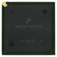
MPC561MZP56 Freescale Semiconductor, MPC561MZP56 Datasheet - Page 435

MPC561MZP56
Manufacturer Part Number
MPC561MZP56
Description
IC MPU 32BIT 56MHZ PPC 388-PBGA
Manufacturer
Freescale Semiconductor
Series
MPC5xxr
Datasheet
1.MPC561MZP56.pdf
(1420 pages)
Specifications of MPC561MZP56
Core Processor
PowerPC
Core Size
32-Bit
Speed
56MHz
Connectivity
CAN, EBI/EMI, SCI, SPI, UART/USART
Peripherals
POR, PWM, WDT
Number Of I /o
64
Program Memory Type
ROMless
Ram Size
32K x 8
Voltage - Supply (vcc/vdd)
2.5 V ~ 2.7 V
Data Converters
A/D 32x10b
Oscillator Type
External
Operating Temperature
-40°C ~ 125°C
Package / Case
388-BGA
Controller Family/series
POWER 5xx
No. Of I/o's
56
Ram Memory Size
31KB
Cpu Speed
56MHz
No. Of Timers
32
Embedded Interface Type
QSPI, SCI, UART
No. Of Pwm Channels
12
Rohs Compliant
No
Processor Series
MPC5xx
Core
PowerPC
Data Bus Width
32 bit
Data Ram Size
32 KB
Interface Type
CAN, JTAG, QSPI, SCI, SPI, UART
Maximum Clock Frequency
40 MHz
Number Of Programmable I/os
56
Number Of Timers
22
Operating Supply Voltage
2.6 V to 5 V
Maximum Operating Temperature
+ 85 C
Mounting Style
SMD/SMT
Minimum Operating Temperature
- 40 C
On-chip Adc
2 (10 bit, 32 Channel)
For Use With
MPC564EVB - KIT EVAL FOR MPC561/562/563/564
Lead Free Status / RoHS Status
Contains lead / RoHS non-compliant
Eeprom Size
-
Program Memory Size
-
Lead Free Status / Rohs Status
No
Available stocks
Company
Part Number
Manufacturer
Quantity
Price
Company:
Part Number:
MPC561MZP56
Manufacturer:
Freescale Semiconductor
Quantity:
10 000
Company:
Part Number:
MPC561MZP56R2
Manufacturer:
Freescale Semiconductor
Quantity:
10 000
- Current page: 435 of 1420
- Download datasheet (11Mb)
10.9.6
Freescale Semiconductor
,
1
10:12
13:27
28:30
Bits
HRESET
HRESET
It is recommended that this field hold values that are the power of 2 minus 1 (e.g., 2
7:9
31
Field
Field
Addr
Dual-Mapping Option Register (DMOR)
DMCS
MSB
Name
DME
—
16
0
AT
—
—
17
1
Reserved
Address type. This field can be used to specify that accesses involving the memory bank are
limited to a certain address space type. These bits are used in conjunction with the ATM bits
in the OR. The default value at reset is to map data only. For a full definition of address types,
refer to
Reserved
Dual-mapping chip select. This field determines which chip-select signal is assigned for dual
mapping.
000 CS0
001 CS1
010 CS2
011 CS3
1xx Reserved
Dual mapping enabled. This bit indicates that the contents of the dual-mapping registers and
associated base and option registers are valid and enables the dual-mapping operation. The
default value at reset comes from the internal data bus that reflects the reset configuration
word. See
information.
0 Dual mapping is not active
1 Dual mapping is active
18
2
Figure 10-26. Dual-Mapping Option Register (DMOR)
Section 9.5.8.6, “Address
19
3
MPC561/MPC563 Reference Manual, Rev. 1.2
Section 10.5, “Dual Mapping of the Internal Flash EEPROM
AM
0000_0000_00
Table 10-11. DMBR Bit Descriptions
1
20
4
21
5
0000_0000_0000_0000
22
6
Types.”
0x2F C144
23
7
—
Description
—
24
8
25
9
10
26
ATM
001
3
11
27
- 1 = 7 [0b111]).
12
28
Array,” for more
13
29
Memory Controller
000
—
14
30
LSB
15
31
10-37
Related parts for MPC561MZP56
Image
Part Number
Description
Manufacturer
Datasheet
Request
R

Part Number:
Description:
MPC5 1K0 5%
Manufacturer:
TE Connectivity
Datasheet:

Part Number:
Description:
MPC5 500R 5%
Manufacturer:
TE Connectivity
Datasheet:

Part Number:
Description:
MPC5 5K0 5%
Manufacturer:
Tyco Electronics
Datasheet:

Part Number:
Description:
MPC5 5R0 5%
Manufacturer:
Tyco Electronics
Datasheet:

Part Number:
Description:
MPC5 50K 5%
Manufacturer:
Tyco Electronics
Datasheet:

Part Number:
Description:
MPC5 1R0 5%
Manufacturer:
Tyco Electronics
Datasheet:
Part Number:
Description:
Manufacturer:
Freescale Semiconductor, Inc
Datasheet:
Part Number:
Description:
Manufacturer:
Freescale Semiconductor, Inc
Datasheet:
Part Number:
Description:
Manufacturer:
Freescale Semiconductor, Inc
Datasheet:
Part Number:
Description:
Manufacturer:
Freescale Semiconductor, Inc
Datasheet:
Part Number:
Description:
Manufacturer:
Freescale Semiconductor, Inc
Datasheet:


