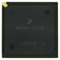
MPC561MZP56 Freescale Semiconductor, MPC561MZP56 Datasheet - Page 431

MPC561MZP56
Manufacturer Part Number
MPC561MZP56
Description
IC MPU 32BIT 56MHZ PPC 388-PBGA
Manufacturer
Freescale Semiconductor
Series
MPC5xxr
Datasheet
1.MPC561MZP56.pdf
(1420 pages)
Specifications of MPC561MZP56
Core Processor
PowerPC
Core Size
32-Bit
Speed
56MHz
Connectivity
CAN, EBI/EMI, SCI, SPI, UART/USART
Peripherals
POR, PWM, WDT
Number Of I /o
64
Program Memory Type
ROMless
Ram Size
32K x 8
Voltage - Supply (vcc/vdd)
2.5 V ~ 2.7 V
Data Converters
A/D 32x10b
Oscillator Type
External
Operating Temperature
-40°C ~ 125°C
Package / Case
388-BGA
Controller Family/series
POWER 5xx
No. Of I/o's
56
Ram Memory Size
31KB
Cpu Speed
56MHz
No. Of Timers
32
Embedded Interface Type
QSPI, SCI, UART
No. Of Pwm Channels
12
Rohs Compliant
No
Processor Series
MPC5xx
Core
PowerPC
Data Bus Width
32 bit
Data Ram Size
32 KB
Interface Type
CAN, JTAG, QSPI, SCI, SPI, UART
Maximum Clock Frequency
40 MHz
Number Of Programmable I/os
56
Number Of Timers
22
Operating Supply Voltage
2.6 V to 5 V
Maximum Operating Temperature
+ 85 C
Mounting Style
SMD/SMT
Minimum Operating Temperature
- 40 C
On-chip Adc
2 (10 bit, 32 Channel)
For Use With
MPC564EVB - KIT EVAL FOR MPC561/562/563/564
Lead Free Status / RoHS Status
Contains lead / RoHS non-compliant
Eeprom Size
-
Program Memory Size
-
Lead Free Status / Rohs Status
No
Available stocks
Company
Part Number
Manufacturer
Quantity
Price
Company:
Part Number:
MPC561MZP56
Manufacturer:
Freescale Semiconductor
Quantity:
10 000
Company:
Part Number:
MPC561MZP56R2
Manufacturer:
Freescale Semiconductor
Quantity:
10 000
- Current page: 431 of 1420
- Download datasheet (11Mb)
Freescale Semiconductor
17:19
20:21
Bits
0:16
22
23
24
25
26
27
28
29
WEBS
TBDIP
LBDIP
Name
SETA
SST
WP
BA
PS
BL
AT
—
Base address. These bits are compared to the corresponding unmasked address signals among
ADDR[0:16] to determine if a memory bank controlled by the memory controller is being
accessed by an internal bus master. (The address types are also compared.) These bits are used
in conjunction with the AM[0:16] bits in the OR.
Address type. This field can be used to require accesses of the memory bank to be limited to a
certain address space type. These bits are used in conjunction with the ATM bits in the OR. Note
that the address type field uses only AT[0:2] and does not need AT3 to define the memory type
space. For a full definition of address types, refer to
Port size
00 32-bit port
01 8-bit port
10 16-bit port
11 Reserved
Short Setup Time – This field specifies the setup time required for this memory region.
0 Normal setup time (like the MPC555)
1 Short Setup Time selected
Note that an external burst access with short setup timing will corrupt any USIU register
load/store if SCCR[EBDF] is not 0b00. Refer to
Write protect. An attempt to write to the range of addresses specified in a base address register
that has this bit set can cause the TEA signal to be asserted by the bus-monitor logic (if enabled),
causing termination of this cycle.
0 Both read and write accesses are allowed
1 Only read accesses are allowed. The CSx signal and TA are not asserted by the memory
Reserved
Burst Length – This field specifies the maximum number of words that may comprise a burst
access for this memory region. This field has an effect only in the case when the burst accesses
are initiated by the USIU (SIUMCR[BURST_EN] =1).
0 Burst access of up to 4 words
1 Burst access of up to 8 words
Write-enable/byte-select. This bit controls the functionality of the WE/BE pads.
0 The WE/BE pads operate as WE
1 The WE/BE pads operate as BE
Toggle-burst data in progress. TBDIP determines how long the BDIP strobe will be asserted for
each data beat in the burst cycles.
Late-burst-data-in-progress (LBDIP). This bit determines the timing of the first assertion of the
BDIP signal in burst cycles.
NOTE: Do not set both LBDIP and TBDIP bits in a region’s base registers; behavior in such cases
is unpredictable.
0 Normal timing for BDIP assertion (asserts one clock after negation of TS)
1 Late timing for BDIP assertion (asserts after the programmed number of wait states)
External transfer acknowledge
0 TA generated internally by memory controller
1 TA generated by external logic. Note that programming the timing of CS/WE/OE strobes may
controller on write cycles to this memory bank. WPER is set in the MSTAT register if a write to
this memory bank is attempted
have no meaning when this bit is set
MPC561/MPC563 Reference Manual, Rev. 1.2
Table 10-8. BR0–BR3 Bit Descriptions
Description
Table
Section 9.5.8.6, “Address
8-9.
Types.”
Memory Controller
10-33
Related parts for MPC561MZP56
Image
Part Number
Description
Manufacturer
Datasheet
Request
R

Part Number:
Description:
MPC5 1K0 5%
Manufacturer:
TE Connectivity
Datasheet:

Part Number:
Description:
MPC5 500R 5%
Manufacturer:
TE Connectivity
Datasheet:

Part Number:
Description:
MPC5 5K0 5%
Manufacturer:
Tyco Electronics
Datasheet:

Part Number:
Description:
MPC5 5R0 5%
Manufacturer:
Tyco Electronics
Datasheet:

Part Number:
Description:
MPC5 50K 5%
Manufacturer:
Tyco Electronics
Datasheet:

Part Number:
Description:
MPC5 1R0 5%
Manufacturer:
Tyco Electronics
Datasheet:
Part Number:
Description:
Manufacturer:
Freescale Semiconductor, Inc
Datasheet:
Part Number:
Description:
Manufacturer:
Freescale Semiconductor, Inc
Datasheet:
Part Number:
Description:
Manufacturer:
Freescale Semiconductor, Inc
Datasheet:
Part Number:
Description:
Manufacturer:
Freescale Semiconductor, Inc
Datasheet:
Part Number:
Description:
Manufacturer:
Freescale Semiconductor, Inc
Datasheet:


