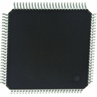
Z16F2811AL20SG Zilog, Z16F2811AL20SG Datasheet - Page 65

Z16F2811AL20SG
Manufacturer Part Number
Z16F2811AL20SG
Description
IC ZNEO MCU FLASH 128K 100LQFP
Manufacturer
Zilog
Series
Encore!® ZNEOr
Specifications of Z16F2811AL20SG
Core Processor
ZNEO
Core Size
16-Bit
Speed
20MHz
Connectivity
EBI/EMI, I²C, IrDA, LIN, SPI, UART/USART
Peripherals
Brown-out Detect/Reset, DMA, POR, PWM, WDT
Number Of I /o
76
Program Memory Size
128KB (128K x 8)
Program Memory Type
FLASH
Ram Size
4K x 8
Voltage - Supply (vcc/vdd)
2.7 V ~ 3.6 V
Data Converters
A/D 12x10b
Oscillator Type
Internal
Operating Temperature
0°C ~ 70°C
Package / Case
100-LQFP
Processor Series
Z16F2x
Core
Zneo
Data Bus Width
16 bit
Data Ram Size
4 B
Interface Type
ESPI, I2C, UART
Maximum Clock Frequency
20 MHz
Number Of Programmable I/os
76
Number Of Timers
4
Operating Supply Voltage
2.7 V to 3.6 V
Maximum Operating Temperature
+ 70 C
Mounting Style
SMD/SMT
Development Tools By Supplier
Z16F2800100ZCOG
Minimum Operating Temperature
0 C
On-chip Adc
10 bit, 12 Channel
For Use With
770-1003 - ISP 4PORT FOR ZILOG ZNEO MCU269-4537 - DEV KIT FOR Z16F ZNEO
Lead Free Status / RoHS Status
Lead free / RoHS Compliant
Eeprom Size
-
Lead Free Status / Rohs Status
Details
Other names
269-4533
Available stocks
Company
Part Number
Manufacturer
Quantity
Price
Company:
Part Number:
Z16F2811AL20SG
Manufacturer:
VISHAY
Quantity:
9 487
Part Number:
Z16F2811AL20SG
Manufacturer:
ZILOG
Quantity:
20 000
- Current page: 65 of 388
- Download datasheet (22Mb)
PS022008-0810
Table 15. External Interface Timing for a Write Operation - ISA Mode
Parameter
T
T
T
T
T
T
T
T
T
T
T
T
T
T
1
2
3
4
5
6
7
8
9
10
11
12
13
14
External Interface Write Timing - ISA Mode
Figure 12
performing a Write operation. In
generator has been configured to provide 1 Wait state during Write operations. The
external WAIT input pin is generating an additional Wait period. As with the normal
mode, the WR signal is fed back from the pin and used on chip to time the removal of the
data signals to ensure proper timing of the data hold.
Abbreviation
XIN Rise to Address Valid Delay
XIN Rise to Address Output Hold Time
XIN Rise to Data Valid Delay
WR Rise to Data Output Hold Time
XIN Rise to CS Assertion Delay
XIN Rise to CS Deassertion Hold Time
XIN Fall to WR Assertion Delay
XIN Fall to WR Deassertion Hold Time
WAIT Input Pin Assertion to XIN Rise Setup Time
WAIT Input Pin Deassertion to XIN Rise Setup Time
XIN Rise to DMAACK Assertion Delay
XIN Rise to DMAACK Deassertion Hold Time
XIN Rise to BHEN or BLEN Assertion Delay
XIN Rise to BHEN or BLEN Deassertion Hold Time
on page 51 and
Table 15
P R E L I M I N A R Y
Figure 12
provide timing information for the external interface
on page 51, it is assumed that the Wait state
Minimum
3
3
3
3
1
1
3
3
Product Specification
Delay (ns)
ZNEO
External Interface
Maximum
Z16F Series
10
10
10
10
10
10
50
Related parts for Z16F2811AL20SG
Image
Part Number
Description
Manufacturer
Datasheet
Request
R

Part Number:
Description:
High Performance Microcontrollers
Manufacturer:
ZiLOG Semiconductor
Datasheet:

Part Number:
Description:
Communication Controllers, ZILOG INTELLIGENT PERIPHERAL CONTROLLER (ZIP)
Manufacturer:
Zilog, Inc.
Datasheet:

Part Number:
Description:
KIT DEV FOR Z8 ENCORE 16K TO 64K
Manufacturer:
Zilog
Datasheet:

Part Number:
Description:
KIT DEV Z8 ENCORE XP 28-PIN
Manufacturer:
Zilog
Datasheet:

Part Number:
Description:
DEV KIT FOR Z8 ENCORE 8K/4K
Manufacturer:
Zilog
Datasheet:

Part Number:
Description:
KIT DEV Z8 ENCORE XP 28-PIN
Manufacturer:
Zilog
Datasheet:

Part Number:
Description:
DEV KIT FOR Z8 ENCORE 4K TO 8K
Manufacturer:
Zilog
Datasheet:

Part Number:
Description:
CMOS Z8 microcontroller. ROM 16 Kbytes, RAM 256 bytes, speed 16 MHz, 32 lines I/O, 3.0V to 5.5V
Manufacturer:
Zilog, Inc.
Datasheet:

Part Number:
Description:
Low-cost microcontroller. 512 bytes ROM, 61 bytes RAM, 8 MHz
Manufacturer:
Zilog, Inc.
Datasheet:

Part Number:
Description:
Z8 4K OTP Microcontroller
Manufacturer:
Zilog, Inc.
Datasheet:

Part Number:
Description:
CMOS SUPER8 ROMLESS MCU
Manufacturer:
Zilog, Inc.
Datasheet:

Part Number:
Description:
SL1866 CMOSZ8 OTP Microcontroller
Manufacturer:
Zilog, Inc.
Datasheet:

Part Number:
Description:
SL1866 CMOSZ8 OTP Microcontroller
Manufacturer:
Zilog, Inc.
Datasheet:

Part Number:
Description:
OTP (KB) = 1, RAM = 125, Speed = 12, I/O = 14, 8-bit Timers = 2, Comm Interfaces Other Features = Por, LV Protect, Voltage = 4.5-5.5V
Manufacturer:
Zilog, Inc.
Datasheet:


