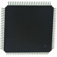
Z16F2811AL20SG Zilog, Z16F2811AL20SG Datasheet - Page 193

Z16F2811AL20SG
Manufacturer Part Number
Z16F2811AL20SG
Description
IC ZNEO MCU FLASH 128K 100LQFP
Manufacturer
Zilog
Series
Encore!® ZNEOr
Specifications of Z16F2811AL20SG
Core Processor
ZNEO
Core Size
16-Bit
Speed
20MHz
Connectivity
EBI/EMI, I²C, IrDA, LIN, SPI, UART/USART
Peripherals
Brown-out Detect/Reset, DMA, POR, PWM, WDT
Number Of I /o
76
Program Memory Size
128KB (128K x 8)
Program Memory Type
FLASH
Ram Size
4K x 8
Voltage - Supply (vcc/vdd)
2.7 V ~ 3.6 V
Data Converters
A/D 12x10b
Oscillator Type
Internal
Operating Temperature
0°C ~ 70°C
Package / Case
100-LQFP
Processor Series
Z16F2x
Core
Zneo
Data Bus Width
16 bit
Data Ram Size
4 B
Interface Type
ESPI, I2C, UART
Maximum Clock Frequency
20 MHz
Number Of Programmable I/os
76
Number Of Timers
4
Operating Supply Voltage
2.7 V to 3.6 V
Maximum Operating Temperature
+ 70 C
Mounting Style
SMD/SMT
Development Tools By Supplier
Z16F2800100ZCOG
Minimum Operating Temperature
0 C
On-chip Adc
10 bit, 12 Channel
For Use With
770-1003 - ISP 4PORT FOR ZILOG ZNEO MCU269-4537 - DEV KIT FOR Z16F ZNEO
Lead Free Status / RoHS Status
Lead free / RoHS Compliant
Eeprom Size
-
Lead Free Status / Rohs Status
Details
Other names
269-4533
Available stocks
Company
Part Number
Manufacturer
Quantity
Price
Company:
Part Number:
Z16F2811AL20SG
Manufacturer:
VISHAY
Quantity:
9 487
Part Number:
Z16F2811AL20SG
Manufacturer:
ZILOG
Quantity:
20 000
- Current page: 193 of 388
- Download datasheet (22Mb)
ESPI Signals
PS022008-0810
Master-In/Slave-Out
Master-Out/Slave-In
Serial Clock
Slave Select
The four ESPI signals are:
•
•
•
•
The following paragraphs describe these signals in both MASTER and SLAVE modes.
The appropriate GPIO pins must be configured using the GPIO alternate function
registers.
The MISO pin is configured as an input in a master device and as an output in a slave
device. Data is transferred to most significant bit first. The MISO pin of a slave device is
placed in a high-impedance state if the slave is not selected. When the ESPI is not enabled,
this signal is in a high-impedance state. The direction of this pin is controlled by the
bit of the ESPI control register.
The MOSI pin is configured as an output in a master device and as an input in a slave
device. Data is transferred to most significant bit first. When the ESPI is not enabled, this
signal is in a high-impedance state. The direction of this pin is controlled by the
of the ESPI control register.
The SCK synchronizes data movement both in and out of the shift register via the MOSI
and MISO pins. In MASTER mode (
serial clock and drives it out via its SCK pin to the slave devices. In SLAVE mode, the
SCK pin is an input. Slave devices ignore the SCK signal unless their SS pin is asserted.
The master and slave are each capable of exchanging a character of data during a sequence
of NUMBITS clock cycles (see NUMBITS field in the
In both master and slave ESPI devices, data is shifted on one edge of the SCK and is
sampled on the opposite edge where data is stable. SCK phase and polarity is determined
by the
The SS signal is a bidirectional framing signal with several modes of operation to support
SPI and other synchronous serial interface protocols. The SLAVE SELECT mode is
selected by the SSMD field of the ESPI mode register. The direction of the SS signal is
Master-In/Slave-Out (MISO)
Master-Out/Slave-In (MOSI)
Serial clock (SCK)
Slave select (SS)
Phase
and
Clkpol
P R E L I M I N A R Y
bits in the
MMEN = 1
ESPI Control Register
), the ESPI’s baud rate generator creates the
Enhanced Serial Peripheral Interface
ESPI Mode Register
on page 193.
Product Specification
ZNEO
on page 195).
Z16F Series
MMEN
MMEN
bit
177
Related parts for Z16F2811AL20SG
Image
Part Number
Description
Manufacturer
Datasheet
Request
R

Part Number:
Description:
High Performance Microcontrollers
Manufacturer:
ZiLOG Semiconductor
Datasheet:

Part Number:
Description:
Communication Controllers, ZILOG INTELLIGENT PERIPHERAL CONTROLLER (ZIP)
Manufacturer:
Zilog, Inc.
Datasheet:

Part Number:
Description:
KIT DEV FOR Z8 ENCORE 16K TO 64K
Manufacturer:
Zilog
Datasheet:

Part Number:
Description:
KIT DEV Z8 ENCORE XP 28-PIN
Manufacturer:
Zilog
Datasheet:

Part Number:
Description:
DEV KIT FOR Z8 ENCORE 8K/4K
Manufacturer:
Zilog
Datasheet:

Part Number:
Description:
KIT DEV Z8 ENCORE XP 28-PIN
Manufacturer:
Zilog
Datasheet:

Part Number:
Description:
DEV KIT FOR Z8 ENCORE 4K TO 8K
Manufacturer:
Zilog
Datasheet:

Part Number:
Description:
CMOS Z8 microcontroller. ROM 16 Kbytes, RAM 256 bytes, speed 16 MHz, 32 lines I/O, 3.0V to 5.5V
Manufacturer:
Zilog, Inc.
Datasheet:

Part Number:
Description:
Low-cost microcontroller. 512 bytes ROM, 61 bytes RAM, 8 MHz
Manufacturer:
Zilog, Inc.
Datasheet:

Part Number:
Description:
Z8 4K OTP Microcontroller
Manufacturer:
Zilog, Inc.
Datasheet:

Part Number:
Description:
CMOS SUPER8 ROMLESS MCU
Manufacturer:
Zilog, Inc.
Datasheet:

Part Number:
Description:
SL1866 CMOSZ8 OTP Microcontroller
Manufacturer:
Zilog, Inc.
Datasheet:

Part Number:
Description:
SL1866 CMOSZ8 OTP Microcontroller
Manufacturer:
Zilog, Inc.
Datasheet:

Part Number:
Description:
OTP (KB) = 1, RAM = 125, Speed = 12, I/O = 14, 8-bit Timers = 2, Comm Interfaces Other Features = Por, LV Protect, Voltage = 4.5-5.5V
Manufacturer:
Zilog, Inc.
Datasheet:


